This thread has been locked.

If you have a related question, please click the "Ask a related question" button in the top right corner. The newly created question will be automatically linked to this question.

LMP90100: PIC LIBRARY

Part Number: LMP90100

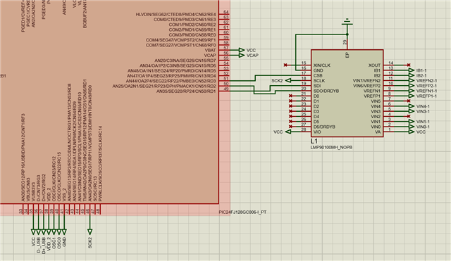
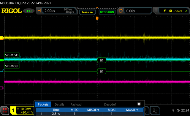
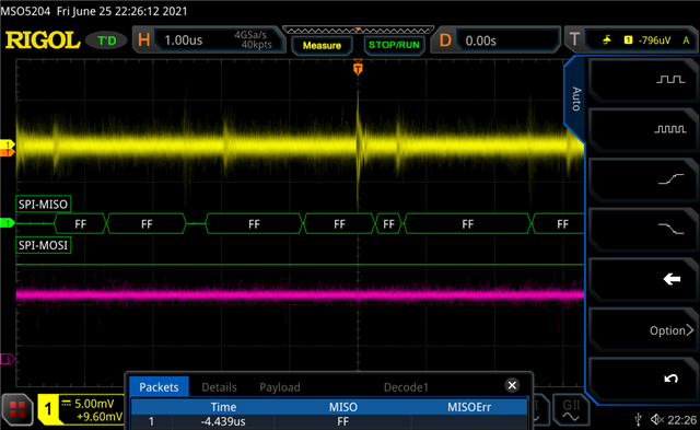
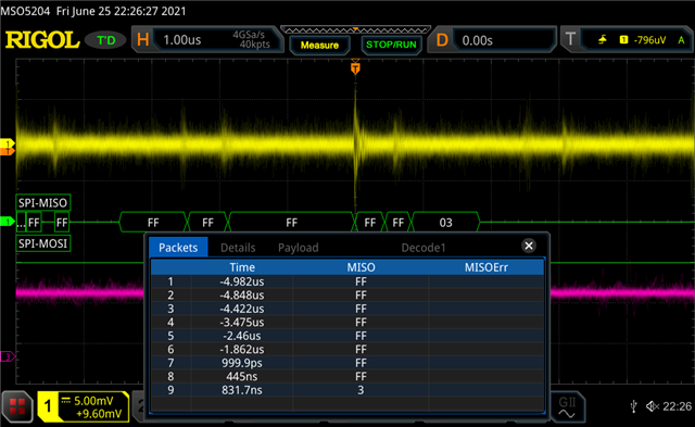
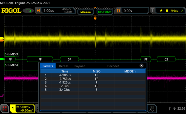
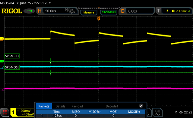
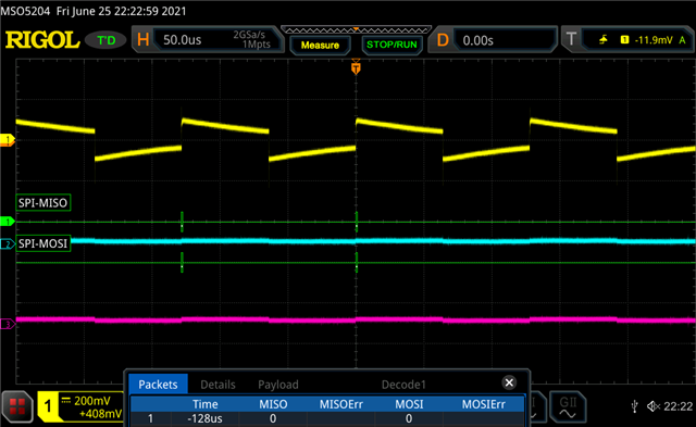
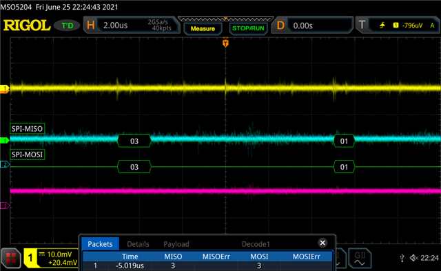
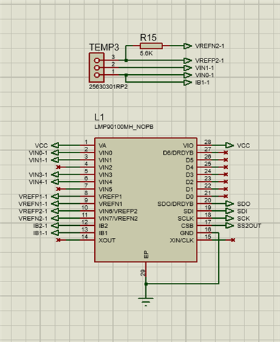
I try to program the LMP90100 with the help of the PIC24F series. I use SPI as a type of communication. However, I have a problem with the fact that the examples for LMP90100 are already written on MSP430. Where can I find the LMP90100 SPI library on pic.
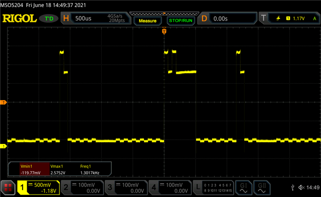
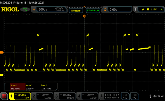
I can write data with LMP90100 e spi, but I have problems reading and making sense of the adc value.
In general, can anyone with information or resources share with me?

  • Hi ASSA,

    I am not aware of any existing PIC code for the LMP90100.

    If you have any specific questions related to the ADC operation or communication, please let me know. However, anything related to the PIC MCU should be directed to the appropriate manufacturer.

    -Bryan

  • Hi Brayn,

    void LMP90100_Write(uint8_t addr, uint8_t value, uint8_t* pURA)
    {
        uint8_t new_URA, inst;
        new_URA = (addr & 0x70) >> 4;
        SS2OUT_SetLow();
        if (*pURA != new_URA)
        {
            inst = 0x10;
            SPI2_Exchange8bit(inst);
            SPI2_Exchange8bit(new_URA);
            *pURA = new_URA;
        }
        inst = 0x00 | 0x00 | (addr & 0x0F);
        SPI2_Exchange8bit(inst);
        SPI2_Exchange8bit(value);
    
        SS2OUT_SetHigh();
    }
    void LMP90100_Read(uint8_t addr, uint8_t* pURA)
    {
        uint8_t x, new_URA, inst;
        new_URA = (addr & 0x70);
        SS2OUT_SetLow();
        if (*pURA != new_URA)
        {
            inst = 0x10;
            SPI2_Exchange8bit(inst);
            SPI2_Exchange8bit(new_URA);
            *pURA = new_URA;
        }
        inst = 0x80 | 0x00 | (addr & 0x0F);
        SPI2_Exchange8bit(inst);
        x = SPI2_Exchange8bit(0);
    
        SS2OUT_SetHigh();
        return x;
    }

    The code I created is as above. But I am not sure of these codes. I am trying to try the first example in the sample codes with these codes, but the value written to the registration address and the value read do not match. When I look at the SPI channels with the help of an oscilloscope, I can see the signal activity.
    I would be glad if you can help.
    Thanks in advance

  • Hi ASSA,

    Have you set up the other SPI signals correctly to the ADC e.g. SCLK, CS, etc.?

    Have you followed the correct timing for SPI commands in the datasheet?

    Please refer to the datasheet for the specifics on how to setup the SPI interface and the correct timing.

    Can you send a schematic of your system so we can see how the inputs and supplies are connected?

    You can also pass along the oscilloscope shots so we can see what commands you are sending to the ADC and how the ADC responds. But without this other requested information, the scope shots will not be valuable.

    -Bryan

  •   SDISDO

    Hi Brayn,

    I added the pictures you requested. I couldn't understand where the problem is in timing.
    Thanks in advance for your help.
  • Hi ASSA,

    Can you please help explain what information you are providing here? The scope shots are not labeled so it is not clear what you are showing.

    Also, the scope shots show the voltage bouncing around quite a bit. If these are the communication lines, it seems like there is quite a bit of noise on the signal lines. You might consider improving your layout or otherwise making sure noise does not enter your system on these sensitive signals. You should also check to make sure you have a solid ground plane or ground connections for all of the digital and analog signals.

    Finally, the schematic you provided has limited information. I cannot see how the analog inputs are connected, nor the supplies, or anything for that matter. Can you include more detail in your next response?

    -Bryan

  • The first osiloscope image is MISO,the other one is MOSI.

    The system is located on the PCB board and the ground line is available on the whole board.What is important to me right now is to write and read values ​​to the LMP90100 registers. I will deal with the analog inputs later
    How can I get the adc measurement values ​​for each channel after writing the required data to the register addresses?
  • Hi ASSA,

    To readback data from the LMP device, you need to follow the guideline shown in the datasheet. There is a quick start section that will help you get up and running (Section 10.1.1). Step 8 in this Quick Start guide points you to the read/write protocol shown in Figure 60 that captures the data from the desired channel (in this case, CH0).

    The read/write protocol shown in Figure 60 details how there are two transactions that must be sent (URA setup and Data Access). If you want to read data, then INST1 = 0x10, URA = 0x1, LRA = 0xA, size = 3 bytes. Then the resulting 3x bytes of data will be output on the SDO pin. Make sure you have CSB asserted during this transaction, and then deassert CSB once the transaction is complete. See Section 9.5.14.2 for an example of reading data with the LMP.

    -Bryan

  • According to what you said,my new code sample is attached.But I was only able to get0 as the adc value.

    1460.Demo.txt
    #include "mcc_generated_files/system.h"
    #include "mcc_generated_files/fatfs/fatfs_demo.h"
    #include "mcc_generated_files/mcc.h"
    
    
    #define FCY 8000000UL
    #include <libpic30.h>
    
    
    static FATFS drive;
    static FIL file;
    
    void LMPW(uint8_t addr1,uint8_t addr2,uint8_t data1,uint8_t data2)
    {
            CS1_SetLow();
            SPI2_Exchange8bit(0x01);
            SPI2_Exchange8bit(0x00);
            SPI2_Exchange8bit(addr1);
            SPI2_Exchange8bit(0x00);
            SPI2_Exchange8bit(0x00);
            SPI2_Exchange8bit(0x01);
            SPI2_Exchange8bit(addr2);
            SPI2_Exchange8bit(data1);
            SPI2_Exchange8bit(data2);
            CS1_SetHigh();
    }
    uint8_t LMPR(uint8_t addr1,uint8_t addr2,uint8_t size)
    {       
            uint8_t reg_read_data;
            CS1_SetLow();
            SPI2_Exchange8bit(0x09);
            SPI2_Exchange8bit(0x00);
            SPI2_Exchange8bit(addr1);
            SPI2_Exchange8bit(0x01);
            SPI2_Exchange8bit(size);
            SPI2_Exchange8bit(addr2);
            reg_read_data=SPI2_Exchange8bit(0x00);
            CS1_SetHigh();
            return reg_read_data;
    }
    void LMPS()
    {
        LMPW(0x00,0x00,0x0c,0x03);
        LMPW(0x00,0x01,0x00,0x01);
        LMPW(0x00,0x03,0x00,0x00);
        LMPW(0x00,0x08,0x00,0x00);
        LMPW(0x00,0x0b,0x00,0x01);
        LMPW(0x00,0x0e,0x00,0x00);
        LMPW(0x00,0x0f,0x00,0x00);
        LMPW(0x01,0x00,0x00,0x02);
        LMPW(0x01,0x01,0x08,0x00);
        LMPW(0x01,0x02,0x00,0x02);
        LMPW(0x01,0x03,0x00,0x00);
        LMPW(0x01,0x04,0x00,0x00);
        LMPW(0x01,0x05,0x00,0x00);
        LMPW(0x01,0x06,0x00,0x00);
        LMPW(0x01,0x07,0x00,0x00);
        LMPW(0x01,0x08,0x00,0x00);
        LMPW(0x01,0x09,0x00,0x00);
        LMPW(0x01,0x0a,0x00,0x00);
        LMPW(0x01,0x0b,0x00,0x00);
        LMPW(0x01,0x0c,0x00,0x00);
        LMPW(0x01,0x0d,0x00,0x00);
        LMPW(0x01,0x0e,0x00,0x00);
        LMPW(0x01,0x0f,0x01,0x08);
        LMPW(0x20,0x00,0x00,0x01);
        LMPW(0x20,0x01,0x04,0x00);
        LMPW(0x20,0x02,0x01,0x03);
        LMPW(0x20,0x03,0x07,0x00);
        LMPW(0x20,0x04,0x02,0x05);
        LMPW(0x20,0x05,0x07,0x00);
        LMPW(0x20,0x06,0x03,0x07);
        LMPW(0x20,0x07,0x07,0x00);
        LMPW(0x20,0x08,0x00,0x01);
        LMPW(0x20,0x09,0x07,0x00);
        LMPW(0x20,0x0a,0x01,0x03);
        LMPW(0x20,0x0b,0x07,0x00);
        LMPW(0x20,0x0c,0x02,0x05);
        LMPW(0x20,0x0d,0x07,0x00);
        LMPW(0x30,0x00,0x00,0x00);
        LMPW(0x30,0x01,0x00,0x00);
        LMPW(0x30,0x02,0x00,0x00);
        LMPW(0x30,0x03,0x08,0x00);
        LMPW(0x30,0x04,0x00,0x00);
        LMPW(0x30,0x05,0x00,0x00);
        LMPW(0x30,0x08,0x00,0x00);
        LMPW(0x30,0x09,0x00,0x00);
        LMPW(0x30,0x0a,0x00,0x00);
        LMPW(0x30,0x0b,0x08,0x00);
        LMPW(0x30,0x0c,0x00,0x00);
        LMPW(0x30,0x0d,0x00,0x00);
        LMPW(0x40,0x00,0x00,0x00);
        LMPW(0x40,0x01,0x00,0x00);
        LMPW(0x40,0x02,0x00,0x00);
        LMPW(0x40,0x03,0x08,0x00);
        LMPW(0x40,0x04,0x00,0x00);
        LMPW(0x40,0x05,0x00,0x00);
        LMPW(0x40,0x08,0x00,0x00);
        LMPW(0x40,0x09,0x00,0x00);
        LMPW(0x40,0x0a,0x00,0x00);
        LMPW(0x40,0x0b,0x08,0x00);
        LMPW(0x40,0x0c,0x00,0x00);
        LMPW(0x40,0x0d,0x00,0x00);
    }
    
    
    int main(void)
    {  
        uint8_t size1,size2,size3,size4,ADC;
        char data1[5],data2[5],data3[5],data8[5];
        char data4[]="\r\nSize1:";
        char data5[]="\r\nSize2:";
        char data6[]="\r\nSize3:";
        char data7[]="\r\nSize4:";
        UINT actualLength;
        CS1_SetHigh();
        SYSTEM_Initialize();
        IO_RE5_SetHigh();
        __delay_ms(1000);
        IO_RE5_SetLow();
        __delay_ms(1000);
        LMPS();
        IO_RE5_SetHigh();
        __delay_ms(1000);
        IO_RE5_SetLow();
        __delay_ms(1000);
        
        
        while (1)
        {
        size1=LMPR(0x01,0x0a,0x00);
        size2=LMPR(0x01,0x0b,0x01);
        size3=LMPR(0x01,0x0c,0x02);
        ADC=LMPR(0x01,0x08,0x00);
        size4=((uint32_t)size1<<16)|((uint16_t)size2<<8)|(size3);
        sprintf(data1,"%d",size1);
        sprintf(data2,"%d",size2);
        sprintf(data3,"%d",size3);
        //sprintf(data8,"%d",size4);
        sprintf(data8,"%d",ADC);
        if( SD_SPI_IsMediaPresent() == false)
        {
            return 0;
        }
        if (f_mount(&drive,"0:",1) == FR_OK)
        {
            if (f_open(&file, "DEMO.TXT", FA_WRITE | FA_OPEN_APPEND ) == FR_OK)
            {   
                f_write(&file, data4, sizeof(data4)-1, &actualLength );
                f_write(&file, data1, sizeof(data1)-1, &actualLength );
                f_write(&file, data5, sizeof(data5)-1, &actualLength );
                f_write(&file, data2, sizeof(data2)-1, &actualLength );
                f_write(&file, data6, sizeof(data6)-1, &actualLength );
                f_write(&file, data3, sizeof(data3)-1, &actualLength );
                f_write(&file, data7, sizeof(data7)-1, &actualLength );
                f_write(&file, data8, sizeof(data8)-1, &actualLength );
                f_close(&file);
            }
    
            f_mount(0,"0:",0);
        }
        IO_RE5_SetHigh();
        __delay_ms(1000);
        IO_RE5_SetLow();
        __delay_ms(1000);
        
        }


        return 1;
    }
    

  • Hi ASSA,

    It is more important to look at the ADC input/output on an oscilloscope or, even better, a logic analyzer, to confirm what is being sent to and received from the ADC. This may very well be a code issue, but I will push back on you the responsibility to review the code since this is not a TI device. However, the logic analyzer will usually help you understand what is going wrong, which will help you determine where in the code the issue might be.

    If you can provide this information I will be happy to review it.

    -Bryan

  • Hi Bryan ,

    I watched the screenshots taken while running the code


    .


  • Hi ASSA,

    The Instruction Byte (INST1) should always be 0x10, even for reads. This is shown in Figure 73. The read/write bit in INST2 still depends on reading or writing, but INST1 is always 0x10.

    I will also assume that you are combining the bits appropriately in the SPI2_Exchange8bit() function, as it appears that each individual transaction is a separate call to that function. For example, the 5 upper bits in the UAB register (all zeroes) are called as one part of that function, while the lower 3 bits of the URA are called separately. I highlighted this in the code below

    I am also not sure why you call "SPI2_Exchange8bit(0x01);" later in the write function. The upper four bits of the INST2 byte should all be zeroes as far as I can tell, since you are writing one byte each time (and bit 4 is always 0).

    Finally, you can take advantage of the streaming functionality if you want to write all of the registers in one call, instead of having to write each register one at a time. This is explained in section 9.5.5. and 9.5.15.1. However, either way will work fine.

    I would suggest first trying to write registers and just read them back to make sure the SPI protocol is working correctly. Then I would move on to trying to read data.

    CS1_SetLow();
    SPI2_Exchange8bit(0x01);
    SPI2_Exchange8bit(0x00); --> these 5 bits should be combined with addr1 to form a single byte that is sent to the ADC
    SPI2_Exchange8bit(addr1);
    SPI2_Exchange8bit(0x00);
    SPI2_Exchange8bit(0x00);
    SPI2_Exchange8bit(0x01); --> why is this 0x01 and not 0x00?
    SPI2_Exchange8bit(addr2);
    SPI2_Exchange8bit(data1);
    SPI2_Exchange8bit(data2);
    CS1_SetHigh();

    -Bryan

  • In line with your suggestions and sample code, your code is edited and the circuit diagram is available below. When I run the code I get 0 as the ADC value.

    #include "mcc_generated_files/system.h"
    #include "mcc_generated_files/mcc.h"
    #include "mcc_generated_files/fatfs/fatfs_demo.h"
    #include "mcc_generated_files/TI_LMP90100.h"
    #include "mcc_generated_files/TI_LMP90100_register_settings.h"
    
    #define FCY 8000000UL
    #include <libpic30.h>
    
    static FATFS drive;
    static FIL file;
    
    void TI_LMP90100_SPIWriteReg(uint8_t addr, uint8_t value, uint8_t *pURA)
    {
      uint8_t new_URA, inst;
      
      new_URA = (addr & 0x70)>>4;                                                   // extract upper register address
      SS2OUT_SetLow();
      //CS1_SetLow();
      
      if (*pURA != new_URA)                                                        // if new and previous URA not same, add transaction 1
      {    
        inst = 0x10;                                                                // Transaction-1
        SPI2_Exchange8bit(inst);
        SPI2_Exchange8bit(new_URA);        
        *pURA = new_URA;                                                            // save new URA
        
      }
      
      inst = 0x00 | 0x00 |(addr & 0x0F);                                            // lower register address
      SPI2_Exchange8bit(inst);
      SPI2_Exchange8bit(value);
      __delay_ms(1);
      //CS1_SetHigh();
      SS2OUT_SetHigh();
    }
    uint8_t TI_LMP90100_SPIReadReg(uint8_t addr, uint8_t *pURA)
    {
      uint8_t x, new_URA, inst;
    
      new_URA = (addr & 0x70)>>4;                                                   // ı upper register address
      SS2OUT_SetLow();
      //CS1_SetLow();
      
      if (*pURA != new_URA)                                                         // if new and previous URA not same, add transaction 1
      {
        inst = 0x10;                                                                // Transaction-1
        
        SPI2_Exchange8bit(inst);
        SPI2_Exchange8bit(new_URA);
        
        
        *pURA = new_URA;                                                           // save new URA
        
     }
     
      inst = 0x80 | 0x00 | (addr & 0x0F);                                           // Transaction-2
      SPI2_Exchange8bit(inst);
      x=SPI2_Exchange8bit(0); 
      //CS1_SetHigh();
      SS2OUT_SetHigh();
    
      return x;
    }
    
    void TI_LMP90100_SPINormalStreamReadADC(uint8_t addr, uint8_t *buffer,uint8_t count, uint8_t *pURA)
    {
      uint8_t i, new_URA, inst;
      
      new_URA = (addr & LMP90100_URA_MASK)>>4;                                     // extract upper register address
      
      SS2OUT_SetLow();
      
      if (*pURA != new_URA)                                                        // if new and previous URA not same, add transaction 1
      {    
        inst = LMP90100_INSTRUCTION_BYTE1_WRITE;                                   // Transaction-1
        
         SPI2_Exchange8bit(inst);
         SPI2_Exchange8bit(new_URA);   
        
        *pURA = new_URA;                                                           // save new URA
        
      }
     
      inst = LMP90100_READ_BIT | LMP90100_SIZE_STREAM | (addr & LMP90100_LRA_MASK);                                         // Transaction-2
      SPI2_Exchange8bit(inst); 
      for(i=0; i<count; i++)
      {    
        *(buffer+i) = SPI2_Exchange8bit(0);
      }
        
      SS2OUT_SetHigh();
          
    }
    void TI_LMP90100_WriteRegSettings(uint8_t *pURA)
    {
     
      TI_LMP90100_SPIWriteReg(TI_LMP90100_RESETCN_REG, 
                              TI_LMP90100_RESETCN_REG_VALUE, pURA);              
      TI_LMP90100_SPIWriteReg(TI_LMP90100_SPI_HANDSHAKECN_REG, 
                              TI_LMP90100_SPI_HANDSHAKECN_REG_VALUE, pURA);         
      TI_LMP90100_SPIWriteReg(TI_LMP90100_SPI_STREAMCN_REG, 
                              TI_LMP90100_SPI_STREAMCN_REG_VALUE, pURA);           
      TI_LMP90100_SPIWriteReg(TI_LMP90100_PWRCN_REG, 
                              TI_LMP90100_PWRCN_REG_VALUE, pURA);                  
      TI_LMP90100_SPIWriteReg(TI_LMP90100_ADC_RESTART_REG, 
                              TI_LMP90100_ADC_RESTART_REG_VALUE, pURA);            
      TI_LMP90100_SPIWriteReg(TI_LMP90100_GPIO_DIRCN_REG, 
                              TI_LMP90100_GPIO_DIRCN_REG_VALUE, pURA);            
      TI_LMP90100_SPIWriteReg(TI_LMP90100_GPIO_DAT_REG, 
                              TI_LMP90100_GPIO_DAT_REG_VALUE, pURA);               
      TI_LMP90100_SPIWriteReg(TI_LMP90100_BGCALCN_REG, 
                              TI_LMP90100_BGCALCN_REG_VALUE, pURA);                 
      TI_LMP90100_SPIWriteReg(TI_LMP90100_SPI_DRDYBCN_REG, 
                              TI_LMP90100_SPI_DRDYBCN_REG_VALUE, pURA);            
      TI_LMP90100_SPIWriteReg(TI_LMP90100_ADC_AUXCN_REG, 
                              TI_LMP90100_ADC_AUXCN_REG_VALUE, pURA);              
      TI_LMP90100_SPIWriteReg(TI_LMP90100_SPI_CRC_CN_REG, 
                              TI_LMP90100_SPI_CRC_CN_REG_VALUE, pURA);             
      TI_LMP90100_SPIWriteReg(TI_LMP90100_SENDIAG_THLDH_REG, 
                              TI_LMP90100_SENDIAG_THLDH_REG_VALUE, pURA);          
      TI_LMP90100_SPIWriteReg(TI_LMP90100_SENDIAG_THLDL_REG, 
                              TI_LMP90100_SENDIAG_THLDL_REG_VALUE, pURA);         
      TI_LMP90100_SPIWriteReg(TI_LMP90100_SCALCN_REG, 
                              TI_LMP90100_SCALCN_REG_VALUE, pURA);                 
      TI_LMP90100_SPIWriteReg(TI_LMP90100_ADC_DONE_REG, 
                              TI_LMP90100_ADC_DONE_REG_VALUE, pURA);               
      
      while (TI_LMP90100_SPIReadReg((TI_LMP90100_CH_STS_REG 
                                     & TI_LMP90100_CH_SCAN_NRDY), pURA));          
      TI_LMP90100_SPIWriteReg(TI_LMP90100_CH_SCAN_REG, 
                              TI_LMP90100_CH_SCAN_REG_VALUE, pURA);                  
      
      TI_LMP90100_SPIWriteReg(TI_LMP90100_CH0_INPUTCN_REG, 
                              TI_LMP90100_CH0_INPUTCN_REG_VALUE, pURA);            
      TI_LMP90100_SPIWriteReg(TI_LMP90100_CH0_CONFIG_REG, 
                              TI_LMP90100_CH0_CONFIG_REG_VALUE, pURA);             
      
      TI_LMP90100_SPIWriteReg(TI_LMP90100_CH1_INPUTCN_REG, 
                              TI_LMP90100_CH1_INPUTCN_REG_VALUE, pURA);            
      TI_LMP90100_SPIWriteReg(TI_LMP90100_CH1_CONFIG_REG, 
                              TI_LMP90100_CH1_CONFIG_REG_VALUE, pURA);              
      
      TI_LMP90100_SPIWriteReg(TI_LMP90100_CH2_INPUTCN_REG, 
                              TI_LMP90100_CH2_INPUTCN_REG_VALUE, pURA);            
      TI_LMP90100_SPIWriteReg(TI_LMP90100_CH2_CONFIG_REG, 
                              TI_LMP90100_CH2_CONFIG_REG_VALUE, pURA);             
      
      TI_LMP90100_SPIWriteReg(TI_LMP90100_CH3_INPUTCN_REG, 
                              TI_LMP90100_CH3_INPUTCN_REG_VALUE, pURA);           
      TI_LMP90100_SPIWriteReg(TI_LMP90100_CH3_CONFIG_REG, 
                              TI_LMP90100_CH3_CONFIG_REG_VALUE, pURA);             
      
      TI_LMP90100_SPIWriteReg(TI_LMP90100_CH4_INPUTCN_REG, 
                              TI_LMP90100_CH4_INPUTCN_REG_VALUE, pURA);            
      TI_LMP90100_SPIWriteReg(TI_LMP90100_CH4_CONFIG_REG, 
                              TI_LMP90100_CH4_CONFIG_REG_VALUE, pURA);             
      
      TI_LMP90100_SPIWriteReg(TI_LMP90100_CH5_INPUTCN_REG, 
                              TI_LMP90100_CH5_INPUTCN_REG_VALUE, pURA);            
      TI_LMP90100_SPIWriteReg(TI_LMP90100_CH5_CONFIG_REG, 
                              TI_LMP90100_CH5_CONFIG_REG_VALUE, pURA);            
       
      TI_LMP90100_SPIWriteReg(TI_LMP90100_CH6_INPUTCN_REG, 
                              TI_LMP90100_CH6_INPUTCN_REG_VALUE, pURA);            
      TI_LMP90100_SPIWriteReg(TI_LMP90100_CH6_CONFIG_REG, 
                              TI_LMP90100_CH6_CONFIG_REG_VALUE, pURA);	       			
     
    }


    int main(void)
    {
      SYSTEM_Initialize();
      UINT actualLength; 
      uint8_t prev_URA,count,addr,read_buf[3]; 
      uint32_t adc_data;
      char data1[3];
      char data[]="\r\n ADC:";
      addr = TI_LMP90100_ADC_DOUT2_REG;                                            // Start Reading from ADC_DOUT2 Register
      count = 3;                                                                   // bytes to read: ADC_DOUT2 - ADCDOUT0
      prev_URA = LMP90100_URA_END;                                                 // Initialize prev_URA to invalid segment 
      TI_LMP90100_WriteRegSettings(&prev_URA);
      CS1_SetHigh();
        IO_RE5_SetHigh();
        __delay_ms(1000);
        IO_RE5_SetLow();
        __delay_ms(1000);
    
      while (1)
      { 
        TI_LMP90100_SPINormalStreamReadADC(addr, read_buf, count, &prev_URA);    // read adc output into read_buf
          
          adc_data = ((uint32_t) read_buf[0] << 16) 
                     | ((uint16_t) read_buf[1] << 8) | read_buf[2];                // form raw adc output data  
          
          sprintf(data1,"%X",adc_data);
          if( SD_SPI_IsMediaPresent() == false)
        {
            return 0;
        }
        if (f_mount(&drive,"0:",1) == FR_OK)
        {
            if (f_open(&file, "DEMO.TXT", FA_WRITE | FA_OPEN_APPEND ) == FR_OK)
            {   
                f_write(&file, data, sizeof(data)-1, &actualLength );
                f_write(&file, data1, sizeof(data1)-1, &actualLength );
                f_close(&file);
            }
    
            f_mount(0,"0:",0);
        }
        IO_RE5_SetHigh();
        __delay_ms(1000);
        IO_RE5_SetLow();
        __delay_ms(1000);
      
      }
    
    
    }


  • Hi ASSA,

    I had asked you to read back the registers before trying to read data. Did you perform this action? If so, what happened?

    Also, it looks like you changed quite a bit in your code. Did you run the code line by line to make the output of each function / variable is as expected? You should also check with an oscilloscope or a logic analyzer to make sure that when you write a register the output from the PIC is what you want it to be. If it isn't, then you have a code error that needs to be resolved.

    That circuit diagram unfortunately does not help very much, as it basically just shows the schematic symbol. It is not clear how the supplies are powered, the decoupling capacitor values, the input filtering, the digital connections, etc.

  • I used the following code to write and read the register.

    And the values ​​I read on the SD card are below.

    #include "mcc_generated_files/system.h"
    #include "mcc_generated_files/mcc.h"
    #include "mcc_generated_files/fatfs/fatfs_demo.h"
    
    
    #define FCY 8000000UL
    #include <libpic30.h>
    
    static FATFS drive;
    static FIL file;
    
    void TI_LMP90100_SPIWriteReg(uint8_t addr, uint8_t value, uint8_t *pURA)
    {
      uint8_t new_URA, inst;
      
      new_URA = (addr & 0x70)>>4;                                                   // extract upper register address
      SS2OUT_SetLow();
      
      
      if (*pURA != new_URA)                                                        // if new and previous URA not same, add transaction 1
      {    
        inst = 0x10;                                                                // Transaction-1
        SPI2_Exchange8bit(inst);
        SPI2_Exchange8bit(new_URA);        
        *pURA = new_URA;                                                            // save new URA
        
      }
      
      inst = 0x00 | 0x00 |(addr & 0x0F);                                            // lower register address
      SPI2_Exchange8bit(inst);
      SPI2_Exchange8bit(value);
      __delay_ms(1);
      
      SS2OUT_SetHigh();
    }
    uint8_t TI_LMP90100_SPIReadReg(uint8_t addr, uint8_t *pURA)
    {
      uint8_t x, new_URA, inst;
    
      new_URA = (addr & 0x70)>>4;                                                   // ı upper register address
      SS2OUT_SetLow();
      
      
      if (*pURA != new_URA)                                                         // if new and previous URA not same, add transaction 1
      {
        inst = 0x10;                                                                // Transaction-1
        
        SPI2_Exchange8bit(inst);
        SPI2_Exchange8bit(new_URA);
        
        
        *pURA = new_URA;                                                           // save new URA
        
     }
     
      inst = 0x80 | 0x00 | (addr & 0x0F);                                           // Transaction-2
      SPI2_Exchange8bit(inst);
      x=SPI2_Exchange8bit(0); 
      
      SS2OUT_SetHigh();
    
      return x;
    }
    void reverse(char s[])
     {
         int i, j;
         char c;
     
         for (i = 0, j = strlen(s)-1; i<j; i++, j--) {
             c = s[i];
             s[i] = s[j];
             s[j] = c;
         }
     }
     
    void itoa(int n, char s[])
     {
         int i, sign;
     
         if ((sign = n) < 0)  /* record sign */
             n = -n;          /* make n positive */
         i = 0;
         do {       /* generate digits in reverse order */
             s[i++] = n % 10 + '0';   /* get next digit */
         } while ((n /= 10) > 0);     /* delete it */
         if (sign < 0)
             s[i++] = '-';
         s[i] = '\0';
         reverse(s);
     }
    
    
    int main(void)
    {
      SYSTEM_Initialize();
      UINT actualLength; 
      uint8_t prev_URA; 
      prev_URA = LMP90100_URA_END;                                                 // Initialize prev_URA to invalid segment 
     
      TI_LMP90100_SPIWriteReg(TI_LMP90100_SPI_DRDYBCN_REG, 
                              0x83, prev_URA);  
      CS1_SetHigh();
      
      IO_RE5_SetHigh();
      __delay_ms(1000);
      IO_RE5_SetLow();
      __delay_ms(1000);
    
      while (1)
      { uint8_t d=TI_LMP90100_SPIReadReg(TI_LMP90100_SPI_DRDYBCN_REG,prev_URA);
        char h[5];
        itoa(d,h);
        char m[]="\r\nSPI_DRDYBCN:";
          if( SD_SPI_IsMediaPresent() == false)
        {
            return 0;
        }
        if (f_mount(&drive,"0:",1) == FR_OK)
        {
            if (f_open(&file, "Demo3.TXT", FA_WRITE | FA_OPEN_APPEND ) == FR_OK)
            {   
                f_write(&file, m, sizeof(m)-1, &actualLength );
                f_write(&file, h, sizeof(h)-1, &actualLength );
                f_close(&file);
            }
    
            f_mount(0,"0:",0);
        }
        IO_RE5_SetHigh();
        __delay_ms(1000);
        IO_RE5_SetLow();
        __delay_ms(1000);
      
      }
    
    
    }


    SPI_DRDYBCN:0   
    SPI_DRDYBCN:0   
    SPI_DRDYBCN:0   
    SPI_DRDYBCN:0   
    SPI_DRDYBCN:0   
    SPI_DRDYBCN:0   
    SPI_DRDYBCN:0   
    SPI_DRDYBCN:0   
    SPI_DRDYBCN:0   
    SPI_DRDYBCN:0   
    SPI_DRDYBCN:0   
    SPI_DRDYBCN:0   
    SPI_DRDYBCN:0   
    SPI_DRDYBCN:0   


  • Hi ASSA,

    Did you step through the code to make sure it functions as you intended? Per the datasheet, are you generating the correct bytes to read and write registers?

    Have you verified the timing is accurate with an oscilloscope or a logic analyzer?

    Have you verified the voltages on the ADC input pins are valid, within specification, and do not droop when the ADC is running?

    Have you verified that the PIC is configured correctly (GPIOs are selected as needed, the correct SPI peripheral is selected if there is more than one, etc.)?

    Until you check on all of these potential issues, I cannot help you further. There are just too many unknowns at this point, and I need you to help verify them before continuing with support. Please read the LMP90100 datasheet carefully and make sure your system follows the specs and requirements outlined in this document.

    Please let me know what you discover after completing / verifying all of these tasks.

    -Bryan

  • Hi Brayn,

    1-Correct codes have been created by referencing the data sheet and sample codes.

    2-As the clock signal is triggered, data is exchanged from MISO and MOSI.

    3-At the moment, I'm just trying to read and write data to the register values. That's why I haven't looked at the ADC pins yet. The power values ​​coming to the LMP90100 provide the necessary conditions.

    4-All the configurations of the PIC are correct and I am sure that the PIC is working. Because the SD card performs the SPI communication, the led blink application and the oled display application. Also, I use a different SPI module of the PIC for the SD card.