Other Parts Discussed in Thread: ADS1118
HI
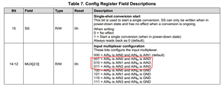
On the hardware connection, we collect three signals, which are respectively connected to ain0, ain1 and ain2, and the signal reference ground is connected to ain3,
The acquisition mode is 001, 010 and 011 in the configuration register,
Sampling rate 128sps, FSR is ± 6.144 V ,Continuous-conversion mode ,ADC mode (default) ,NOP[1:0] =01。
In practical application, we change the configuration register config register every 10 ms and read the data of each channel,
However, it is found that the data of each channel is in series with each other.
Ain1 will display the signal input values of ain1 and ain3 at intervals, ain2 will display the signal input values of ain2 and ain1 at intervals, and ain3 will display the signal input values of ain3 and ain2 at intervals.
When the change interval of the configuration register and the sampling read interval are increased to 100ms, the phenomenon disappears, and the sampling data is stable and accurate.
What is the reason for this phenomenon? Is there any problem with software or hardware? 100ms for the actual sampling rate is too large to meet the requirements
Thanks!