This thread has been locked.

If you have a related question, please click the "Ask a related question" button in the top right corner. The newly created question will be automatically linked to this question.

ADS8166: What is the tolerance on the Vrefby2 buffer output?

Part Number: ADS8166

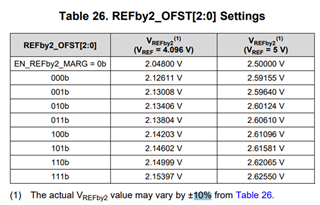
The DS isn't clear, but the note below DS table 26 says: "(1) The actual VREFby2 value may vary by ±10% from Table 26."

Does this mean that the min/max of the Vrefby2 is ±10% from Vref/2? I assume this is not correct. Please provide the accuracy of the Vrefby2 output which would be a combination of the divider tolerance and offset voltage. If this is trimmed during production, is it reflected in the DS somewhere and I'm just missing it? Thanks- Mark.

  • Hi Mark,

    We do not specify a min/max value in the datasheet, just a mean value.


    The VREFby2 output in ADS816x has a mean of REF/2.  The +/-10% comment is for the margining feature of REF/2. The customer can adjust the output of the VREFby2 buffer to get slightly higher output voltages – this adjustment has 10% tolerance.


    For example, if REFby2_OFST[2:0]=111b, Vrefby2 increases from 2.5V to 2.62550V for Vref=5V.  This offset of 0.1255V (2.62550-2.5) has a tolerance of +/-10%, or 0.11295V to 0.13805V.

    Best,

    Zak