


Part Number: ADS54J60
we use a ADS54J60 PCB designed by ourself,and use zcu102 to process。jesd204b IP is already worked,and the clock is worked,but after ADS54J60 Initialization Sequence by SPI doesn't get the right output。
SPI is right, out ADS54J60 Initialization Sequence is:
| Apply a hardware reset by pulsing pin 48 (low → high → low) |
cmd(0,0x81);
cmd(0x4001,0);
cmd(0x4002,0);
cmd(0x4003,0);
cmd(0x4004,0x68);
cmd(0x60f7,1);
cmd(0x6000,1);
cmd(0x6000,0);
mdelay(200);
cmd(0x0011,0x80);
cmd(0x0059,0x20);
cmd(0x4003,0);
cmd(0x4004,0x69);//
cmd(0x6000,0x80);
//JESD link is configured with LMFS = 8224 by default with no decimation.
cmd(0x4003,0);
cmd(0x4004,0x6A);
//JESD link is configured with LMFS = 8224 by default with no decimation.
cmd(0x6017,0x40);
cmd(0x6017,0x00);
cmd(0x4003,0);
cmd(0x4004,0x68);
//JESD link is configured with LMFS = 8224 by default with no decimation
cmd(0x6000,1);
cmd(0x6000,0);
cmd(0x4003,0);
cmd(0x4004,0x69);
cmd(0x6002,0x40);//K28.5
cmd(0x6006,0x0F);//(choose the value of K
reset jesd204b的IP核
and then we read the reg from ADS54J60:
read back
Select the Analog Page
addr20:0
addr21:0
addr22:0
addr26:0
addr4F:0
addr53:0
addr55:0
addr59:20
68--Select the main digital page of the JESD bank
addrF7:0
addr0:0
69--Select the JESD digital page
addr0:80
addr1:1
addr2:0
addr3:0
addr5:0
addr6:F
addr7:9
addr16:80
addr31:0
addr32:0
6A--Select the JESD analog page
addr16:0
addr12:0
addr17:0
and final waveform like this
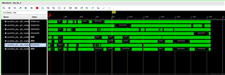
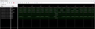

before reset(Apply a hardware reset by pulsing pin 48 (low → high → low)),8 lane receive 0,after reset, we get the waveform just like above waveform,it seems mean that the Initialization for ADS54J60 doesn't work,but the reg readback is right。
here's the params:
LMFS=8266
K=16
the clock for ADS54J60,CLKIN=960M,sysref=3M,
FPGA part,lanerate=4.8G,refclk=120M,sysref=3M
can you help me for this? what's wrong and how to check or resolve it?


