- Ask a related questionWhat is a related question?A related question is a question created from another question. When the related question is created, it will be automatically linked to the original question.
This thread has been locked.
If you have a related question, please click the "Ask a related question" button in the top right corner. The newly created question will be automatically linked to this question.
Hello,
I want to know how to configure Arria10 FPGA JESD204B of TSW14J57EVM.
Our test configuration:
EVM: AFE7950EVM <-> TSW14J57EVM
Latte script: AFE79xx_EVM_Mode7.py
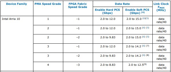
[Intel JESD 204B IP User Guide for Intel Arria10]
URL: https://www.intel.com/content/dam/www/programmable/us/en/pdfs/literature/ug/ug_jesd204b.pdf
In the Page 14
2.7. Performance and Resource Utilization Table 8. JESD204B Intel FPGA IP Performance

According to above mode 7 TX, Input rate should be 737.28Msps. I’m confusing because I though Arria10 can support Input Rate up to 300 Mhz. Intel JESD204B IP User Guide says ‘Max Link Clock = data rate/40 = 15Gbps/40‘ and it is 375 MHz. It is much less than 737.28 Msps.
Can you please tell me how my thinking is wrong?
Best regards.
Hi Louis,
The data rate of each I and Q channel is 737.28 MSPS and each sample has 16 bits. This data of each I or Q channel is sent over a 32-bit parallel bus to the JESD block of Arria10. Because of this parallelization, actual data rate of each bit in this 32-bit bus would be 737.28*16/32 = 368.64 Mbps.
After 8b/10b encoding, data rate per each I or Q channel is 737.28*16*(10/8) = 14745.6 Mbps. But this data is sent to SERES block over a 40-bit parallel bus to keep the data rate of each bit at 14745.6/40 = 368.64 Mbps. This is why link clock is set to 368.64MHz.
In SERDES block this data gets serialized on to a SERDES lane running at 14745.6 Mbps.
Regards,
Vijay