This thread has been locked.

If you have a related question, please click the "Ask a related question" button in the top right corner. The newly created question will be automatically linked to this question.

DAC34H84EVM: J10/J11 CDCE62005 LVDS clock output error

Part Number: DAC34H84EVM
Other Parts Discussed in Thread: CDCE62005, DAC34H84, DAC34SH84

Dear Team,

My customer is evaluating the DAC34H84EVM with the DAC348x EVM Software GUI. They want to set LVDS clock output as 207.36MHz from J10/J11 pins of the DAC34H84EVM which are U4P/U4N pins of the CDCE62005. The DAC34H84EVM has the 19.2MHz TCXO which is inputted into SEC REF+ pin of the CDCE62005.
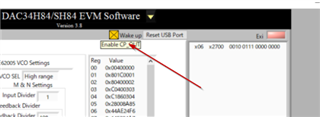
They set the GUI as attached, but they got 211.29MHz LVDC clock output from J10/J11 pins of the DAC34H84EVM.
Could you advise them on how to set up the GUI to get the correct 207.36MHz LVDC clock output from J10/J11 pins of the DAC34H84EVM?

CDCE Output Settings, Y4 FPGACLK2 is settings for J10/J11 pins of the DAC34H84EVM.

I look forward to your reply.
Thank you.

Best Regards,

Koshi Ninomiya

  • Hi Koshi-san,

    Please advise the customer to toggle the "wake-up" button. This will calibrate out the VCO tune for the CDCE62005.

    Please also ask the customer to send their configuration file. We may need to get Clock team to support this configuration. Thanks. 

  • Hi Kang-san,

    The customer tried to toggle the "wake-up" button at the setting or after loading the configuration file, but the phenomenon was not improved.

    Please review attached configuration files from the customer.
     - DAC_config_CDC.txt  :  Configuration file for CDCE62005 device only
     - DAC_config_full.txt  :  Configuration file including DAC34H84 device

    They found a issue. When they set the DAC register "x02", DAC32H84 device settings became default value, although CDCE62005 device settings was kept as the configuration file.
    When they read the register value after loading "DAC_config_full.txt", it became different value as the following,
     - DAC_config_full_Read_after_Load.txt

       x00	   x0000
       x01	   x0000
       x02	   x0000
       x03	   x0000
       x04	   xE5B1
       x05	   x3A60
       x06	   x3100
       x07	   x0000
       x08	   x0000
       x09	   x0000
       x0A	   x0000
       x0B	   x0000
       x0C	   x0000
       x0D	   x0000
       x0E	   x0000
       x0F	   x0000
       x10	   x0000
       x11	   x0000
       x12	   x0000
       x13	   x0000
       x14	   x0000
       x15	   x0000
       x16	   x0000
       x17	   x0000
       x18	   x0007
       x19	   x0000
       x1A	   x0020
       x1B	   x0000
       x1C	   x0000
       x1D	   x0000
       x1E	   x0000
       x1F	   x0000
       x20	   x0000
       x22	   x0000
       x23	   x0000
       x24	   x0000
       x25	   x0000
       x26	   x0000
       x27	   x0000
       x28	   x0000
       x29	   x0000
       x2A	   x0000
       x2B	   x0000
       x2C	   x0000
       x2D	   x0000
       x2E	   x0000
       x2F	   x0000
       x30	   x0000
       x7F	   x0001
    CDCE62005 Registers
    Freq:19.200000MHz
    Address	Data
    00		00400000
    01		81860301
    02		81860302
    03		C1860303
    04		C1860304
    05		28001A95
    06		44AF24F6
    07		145294A7
    08		20001808

       x00	   x019F
       x01	   x0402
       x02	   x7082
       x03	   xA000
       x04	   x0000
       x05	   x0000
       x06	   x0000
       x07	   xD8FF
       x08	   x0000
       x09	   x8000
       x0A	   x0000
       x0B	   x0000
       x0C	   x0000
       x0D	   x0000
       x0E	   x0000
       x0F	   x0000
       x10	   x0000
       x11	   x0000
       x12	   x0000
       x13	   x0000
       x14	   x0000
       x15	   x0000
       x16	   x0000
       x17	   x0000
       x18	   x2460
       x19	   x1034
       x1A	   x1800
       x1B	   x0800
       x1C	   x0000
       x1D	   x0000
       x1E	   x1111
       x1F	   x1140
       x20	   x1101
       x22	   x1B1B
       x23	   xFFFF
       x24	   x0000
       x25	   x0000
       x26	   x0000
       x27	   x0000
       x28	   x0000
       x29	   x0000
       x2A	   x0000
       x2B	   x0000
       x2C	   x0000
       x2D	   x0004
       x2E	   x0000
       x2F	   x0000
       x30	   x0000
       x7F	   x0001
    CDCE62005 Registers
    Freq:19.200000MHz
    Address	Data
    00		00400000
    01		81860301
    02		81860302
    03		C1860303
    04		C1860304
    05		28001A95
    06		44AF24F6
    07		145294A7
    08		20001808

       x00	   x0000
       x01	   x0000
       x02	   x0000
       x03	   x0000
       x04	   xFFFF
       x05	   x267E
       x06	   x3300
       x07	   x0000
       x08	   x0000
       x09	   x0000
       x0A	   x0000
       x0B	   x0000
       x0C	   x0000
       x0D	   x0000
       x0E	   x0000
       x0F	   x0000
       x10	   x0000
       x11	   x0000
       x12	   x0000
       x13	   x0000
       x14	   x0000
       x15	   x0000
       x16	   x0000
       x17	   x0000
       x18	   x0007
       x19	   x0000
       x1A	   x0020
       x1B	   x0000
       x1C	   x0000
       x1D	   x0000
       x1E	   x0000
       x1F	   x0000
       x20	   x0000
       x22	   x0000
       x23	   x0000
       x24	   x0000
       x25	   x0000
       x26	   x0000
       x27	   x0000
       x28	   x0000
       x29	   x0000
       x2A	   x0000
       x2B	   x0000
       x2C	   x0000
       x2D	   x0000
       x2E	   x0000
       x2F	   x0000
       x30	   x0000
       x7F	   x0001
    CDCE62005 Registers
    Freq:19.200000MHz
    Address	Data
    00		00400000
    01		81860301
    02		81860302
    03		C1860303
    04		C1860304
    05		28001A95
    06		44AF24F6
    07		145294A7
    08		20001808

    Thank you.

    Best Regards,

    Koshi Ninomiya

  • Hi Koshi-san,

    Please inquire also with the clock team on this. They are best at answering CDCE62005 questions. Thank you.

    As a reference, you may ask the customer to refer to example DAC34SH84 configurations with on-chip PLL settings for the CDCE62005.

    C:\Program Files (x86)\Texas Instruments\DAC348x\EVM Configuration File Released\DAC34SH84\Example CDCE62005 PLL Configuration

    Thank you

  • Koshi-san,

    0x02 register has 4 wire SPI setting. They probably set the wrong value and therefore not reading back properly. Please ask the customer to try the files listed above to have a reference point in the modification. Thank you.

  • Hi Kang-san,

    The CDCE62005 LVDS output error was solved during discussing with the clock team as follow,

    CDCE62005: DAC34H84EVM J10/J11 LVDS clock output error (2)

    The remaining issue is this,
    *******************************************************
    They found a issue. When the serial interface, 4bit interface was enabled, when they set the DAC register "x02", DAC32H84 device settings became default value, although CDCE62005 device settings was kept as the configuration file.
    When they read the register value after loading "DAC_config_full.txt", it became different value as the following,
     - DAC_config_full_Read_after_Load.txt

       x00	   x0000
       x01	   x0000
       x02	   x0000
       x03	   x0000
       x04	   xFFFF
       x05	   x267E
       x06	   x3300
       x07	   x0000
       x08	   x0000
       x09	   x0000
       x0A	   x0000
       x0B	   x0000
       x0C	   x0000
       x0D	   x0000
       x0E	   x0000
       x0F	   x0000
       x10	   x0000
       x11	   x0000
       x12	   x0000
       x13	   x0000
       x14	   x0000
       x15	   x0000
       x16	   x0000
       x17	   x0000
       x18	   x0007
       x19	   x0000
       x1A	   x0020
       x1B	   x0000
       x1C	   x0000
       x1D	   x0000
       x1E	   x0000
       x1F	   x0000
       x20	   x0000
       x22	   x0000
       x23	   x0000
       x24	   x0000
       x25	   x0000
       x26	   x0000
       x27	   x0000
       x28	   x0000
       x29	   x0000
       x2A	   x0000
       x2B	   x0000
       x2C	   x0000
       x2D	   x0000
       x2E	   x0000
       x2F	   x0000
       x30	   x0000
       x7F	   x0001
    CDCE62005 Registers
    Freq:19.200000MHz
    Address	Data
    00		00400000
    01		81860301
    02		81860302
    03		C1860303
    04		C1860304
    05		28001A95
    06		44AF24F6
    07		145294A7
    08		20001808

    *****************************************************

    Do you understand cause of this issue?
    Thank you.

    Best Regards,

    Koshi Ninomiya

  • Hi Koshi-san

    Please keep the DAC34SH84 programmed as 3-wire mode (in register 0x02). This is how the example configuration files are done in the GUI. 

  • Hi Kang-san,

    Thank you for your support. The customer was able to resolve the issue of failing to read register information from the GUI by setting the 3-wire mode.

    Best Regards,

    Koshi Ninomiya