This thread has been locked.

If you have a related question, please click the "Ask a related question" button in the top right corner. The newly created question will be automatically linked to this question.

DAC80508:Failed to read device ID

Part Number: DAC80508

Hello! I am using dac80508evm to connect my microcontroller, i.e. CS, SCLK, SDO, SDI, GDN and vio (3.3V), with external VDD of 5V.

At present, I have written the SPI program about microcontroller. I want to start with reading device ID, but it has not been successful.

I'd like to ask you a few questions:

1. What steps should be taken before reading ID( I know that I need to send 0x81 00 00, 0x00 00 00 to read the device. Are there any other operations before sending the command?)

2. What should be configured to satisfy the sequence diagram?

3. After I provide Vdd and vio, is the power on completed? Can SCLK be displayed directly? I didn't see it on an oscilloscope.

4. What initialization does dac80508 need?

I am a beginner in this area, many problems may not be very mature, hope to get your help, thank you!

Best wishes!

  • Hello,

    1. The SDO bit needs to be enabled in the CONFIG register at register address 0x03 by writing 0x0000 before any registers can be read from the DAC. Depending on the SPI mode you have configured on your microcontroller, you may need to enable the FSDO bit as well by writing 0x0400 to register 0x03. 
    2. The DAC samples data on the falling edge of SCLK. SPI on your microcontroller needs to be configured to shift data on the rising edge and sample on the falling edge. It may be easiest to write to the CONFIG register to power up/down the internal reference. Make sure JP3 on the DAC80508EVM is removed so you are not shorting he 5V external reference on the EVM to the internal reference. If you see the reference update when you send the command from your microcontroller, then you will know you have correctly configured SPI.
    3. No, SCLK is only generated when a read or a write is initiated by the microcontroller. The DAC does not supply an SCLK so you will not see the SCLK when you power on the DAC until the microcontroller sends a read or write command. 
    4. This depends on the settings you need to configure. You will likely need to configure the CONFIG register (0x03) to set up the SDO pin for reading and power up or down the internal reference, the GAIN register (0x04) to divide the reference and set the output gain, and the DACx registers (0x08 to 0x0F) to set the DAC outputs. 

    Best,

    Katlynne Jones

  • Hello, thank you very much for your valuable advice. I successfully read the device ID according to your operation steps, but I encountered some confusion when outputting voltage.

    The equipment configuration is as follows: (not shown is the default configuration) VDD = vio = 3.3V

    0x03 0x00 0x00

    0x04 0x01 0xFF

    0x0A 0x80 0x00

    0x0B 0x66 0x66

    0x0C 0x08 0x00

    0x0D 0x04 0x00

    0x0E 0x00 0x60

    0x0F 0x00 0x50

    Question 1. I found that the difference between the actual output voltage value and the theoretical value is 3-5mv. The voltage values are DAC2 = 1.245v, DAC2 = 0.996v, dac3 = 78.5mv, dac4 = 39.5mv and dac5 = 4mv respectively. Is this a normal phenomenon?

    Question 2. My chip is dac80508m. If a DAC register is not assigned, will it maintain zero level or intermediate level?

    Question 3. If I want to output a voltage value similar to the pulse form, for example, keep the output 4mv voltage for 2.5ms and the output 0mV voltage for 7.5ms, and then cycle repeatedly. So, can I use the timer to complete it? Does this have anything to do with SCLK clock? Do you have any suggestions for the functions I want to implement?

    I look forward to hearing from you.

    Best wishes!

  • Hello,

    1. 3-5mV is a reasonable amount of error. The internal reference has a ±5 mV maximum initial accuracy, meaning that at full scale the output could be up to 5mV off. The DAC80508 has a total unadjusted error of 0.1% full scale range (FSR), meaning that the output could be up to 2.5mV off with a 2.5V reference. The TUE does not include the error due to the reference, so this could add up to a few millivolts. 
    2. The default value for the DAC80508M is mid-scale (0x8000). If the DAC register is not set by you after each power-up, then the output will remain at mid-scale. 
    3. No, SCLK is only used for the SPI communication to the device. You would have to use your microcontroller to write to the DAC outputs after a 2.5ms delay. I would suggest a while loop that sets the DAC output to 4mV via SPI, waits 2.5ms, set the DAC output to 0mV via SPI, wait 2.5ms, and repeat. 

    Best,

    Katlynne Jones

  • Hello, thank you for your patient reply.

    The strange thing is that if I set the DAC output value to 0mV, there will be 1mV error in the measured reading. Is there a way to solve this?

    thank you

    Yue

  • What I am worried about is that the DAC output voltage changes rapidly after 2.5ms. Will such repetition have any impact on the chip itself? Or will the output value remain stable for a long time?

    I tried to control the time of two voltage values at 25ms and 75ms. When reading with the voltmeter, I found that the value has remained unchanged at the middle voltage value of 4m and 0mV. Is this because the reflection of the oscilloscope is not so sensitive?

    thank you!

  • Hi Yue Wang,

    I can understand from thread that you are trying to generate 4mV , pulse train with 25% duty cycle.

    Just clarify are you measuring using oscilloscope or voltmeter ? recommended oscilloscope measurement with short Ground lead since long lead create additional noise coupling and you will loose actual data.

    Share the oscilloscope screen shot of output, it will help us to understand issue.   

  • Hello, the voltmeter cannot be tested. I'm looking at the waveform with an oscilloscope.

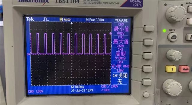
    When the voltage is set to 0xFFFF, i.e. 2.5V, the oscilloscope result is as shown in Figure 1: it seems to be correct;

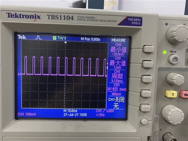
    When the voltage is set to 0x6666, i.e. 99.9mv, the oscilloscope result is shown in Figure 2: it seems to be correct;

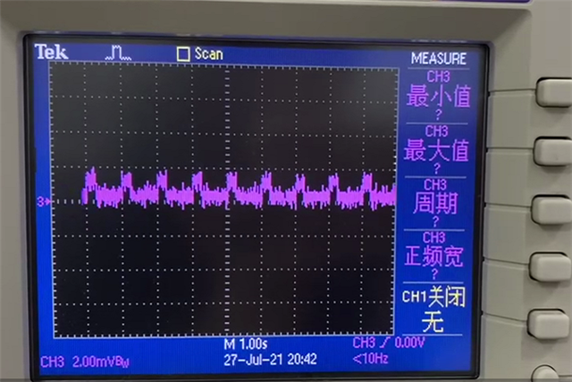
    When the voltage is set to 0x00FC, i.e. 10mv, the oscilloscope results are shown in Figure 3: the maximum and minimum voltages can not be read, and the waveform is subject to many burr interference;

    It can't be read out at 4MV. Is this because of the problem of my oscilloscope model?

    Thanks!

  • Hi,

    I think oscilloscope can read 4mV with noise . Calibrate probe cable and try to measure lower amplitude.

    Also,   total unadjusted error of .1 % will introduce 2.5mV + reference error , offset error. . It seem your measurement closer to expected.