This thread has been locked.

If you have a related question, please click the "Ask a related question" button in the top right corner. The newly created question will be automatically linked to this question.

ADS131E08EVM-PDK: Gerber files for ADS131E08EVM PDK

Part Number: ADS131E08EVM-PDK

Hi Ryan,

   I had earlier asked a query regarding the Gerber files for ADS131E08EVM PDK through this forum. I had received the same from you. 

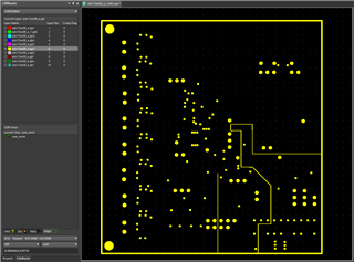
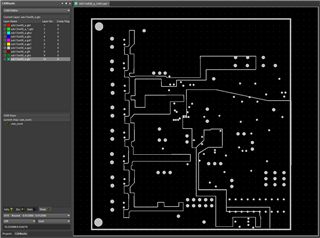
We reviewed these Gerber files again using Altium and observed that there are no copper fills in the inner layers. They are expected to be power/ground planes. Could you please confirm regarding this?

Can TI share the design files for the ADS131E08EVM PDK? Alternatively, can we have a call over teams/zoom/meet wherein we can show you what we are saying.

Regards,

Girish

  • Hello Girish,

    The internal layers are negative plane layers. This means that where you see lines or polygon fills, there is actually no copper. All of the "blank" space between the lines will actually be copper. These are the same layout prints included at the end of the ADS131E08EVM-PDK User Guide. In the future, perhaps we should note that these are negative layers to make it more clear.

    Internal Layer 1 (GND):


    Internal Layer 2 (Power):

    Regards,

    Ryan

  • Thanks Ryan, that explains. Yes, perhaps it would be helpful to note in the EVM guide that these are negative.

    And while its still ok to have the negative layers in the documentation, the actual gerber database should not contain a negative layer. Since, if it goes to a fabricator without any instructions, the resulting board may not work.

    Regards,

    Girish

  • Girish - these are the same gerbers we use for fabrication. We have nothing else to provide.