Part Number: DAC81416EVM
DAC81416: Configuration added here
I used reference code. Send and receive through SPI interface okay.
but problem is send data not getting on DAC out pins.
Please can any one help.
void Dac_Config(void)
{
GPIO_WritePin(DAC_RESETn, CLEAR);
/* Delay for a bit */
DELAY_US(1000); // 1msec
GPIO_WritePin(DAC_RESETn, SET);
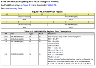
/* DACRANGEn Register A Range: +/- 20V */
dac_init_steps(0x0acccc);
dac_init_steps(0); /* Receive bytes */
/* DACRANGEn Register B Range: +/- 20V */
dac_init_steps(0x0bcccc);
dac_init_steps(0); /*Receive bytes */
/* DACRANGEn Register C Range: +/- 20V */
dac_init_steps(0x0ccccc);
dac_init_steps(0); /* Receive bytes */
/* DACRANGEn Register D Range: +/- 20V */
dac_init_steps(0x0dcccc);
dac_init_steps(0); /* Receive bytes */
/* Power-up device */
dac_init_steps(0x030a84);
/* Power up all channels */
dac_init_steps(0x090000);
/* Enable Broadcast for all channels */
dac_init_steps(0x05ffff);
/* Write code to all channels */
dac_init_steps(0x0fffff);
}
Then sending continues
void loop(void)
{
dacWrite(0x7fff);
/* Delay for a bit */
DELAY_US(1000);// 1msec req
dacWrite(0xffff);
}
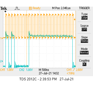
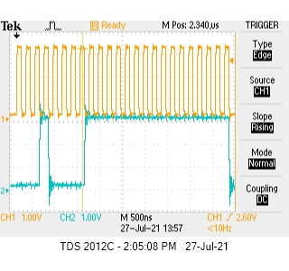
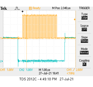
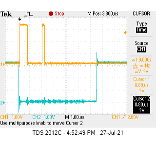
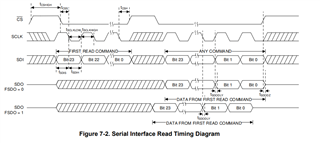
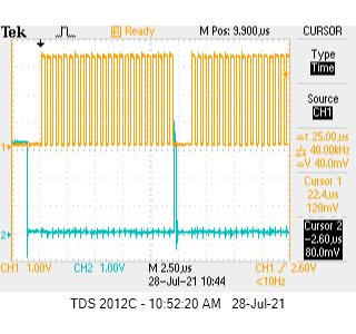
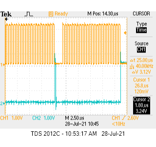
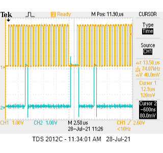
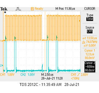
When i am trying to read DEVISE ID and version MISO signal is disturbed.
Note: LDAC and CLR not used.
Giving input supplies
J7.3 ---- GND
J7.4-----VIO-----5V
J7.5-----VDD/VAA-----5V
J7.6 -----VSS-------GND
J7.7-------VCC------30V