This thread has been locked.

If you have a related question, please click the "Ask a related question" button in the top right corner. The newly created question will be automatically linked to this question.

ADS1299: BIAS_SENS signals source

Part Number: ADS1299

Hi TI Team and fellows,

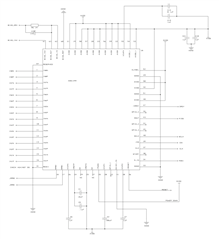
I have a few EEG test boards using closed loop RLD for CMR improvement. This board is used to measure EEG on a subject using referential mode with SRB1 on. All negative electrodes and SRB2 have no connection. In the firmware enabling BIAS_SENSN causes all signals to become railed due to failure of RLD loop.

My question is that:

Is the BIAS_SENS signal generated from PGAP and PGAN, as it seems from the datasheet or is it generated from the INxP and INxN? If it is generated from PGAP and PGAN then the RLD loop should not fail as PGAN is not floating. Can you guys reproduce this error?

Looking forward to the response.

  • Hi Umair,

    Welcome to the E2E forum and thanks for the post !!!

    The BIAS_SENS will enable the switches that connect the BIAS amplifier inverting input to the output of the PGAP and PGAN (see Figure 38). Depending on the number of outputs connected to the circuits, the DC gain of the bias amplifier may vary. Therefore, it is essential to maintain the proper gain so that the bias amplifier will not saturate when multiple outputs are connected. I have listed the FAQ below for your reference.

    [FAQ] ADS129x: How do I calculate the DC gain of the RLD or BIAS amplifier?

    Thanks

    -TC

  • Thanks TC for the quick response,

    Based on figure-58, indeed it seems that BIAS_SENS will enable switches that connect output of PGAP and PGAN to the BIAS_INV.

    However, if that is the case, then it is unclear why using SRB1 should generate any different results from the fully differential mode. As we only route PGAN from SRB1 instead of INxN

    Here is ADS operating circuit we used:

    In case of referential mode i.e. common negative connected to SRB1 all signals become railed when BIAS_SENSN is enabled. However, if differential signals are applied to each channel, this does not happen.

    To verify, if the Bias Amplifier gain was the problem, we conducted tests using 1~8 channels, disabling other channels  Power, Bias Sensing etc. however, results remain similar. Also, a modified board was tested which included 1M RF resister and 1nF CF capacitor for Bias Amplifier feedback which would reduce the amplifier gain, however, results were still similar.

    Regards,

    Umair Usman

  • Hi Umair,

    Thanks for the update.

    There is no difference in connecting each channel differentially through INxN pin or with the SRB1 pin. The SRB1 pin helps simplify the INxN pin's connection in the referential montage mode by connecting all the INxN pins internally.

    You can verify the functionality of the BIAS_DRV circuitry feedback loop by applying a known signal to the INxP and SRB1 inputs. What are the ADC outputs when you disconnect the BIAS_SENS switches to the PGA and setting the BIAS_DRV to the common-mode voltage? For debugging, you can measure the BIAS_DRV signal output voltage with and without the channel feedback. A large DC voltage on the inputs with a large PGA gain can cause the PGA to saturate and the output to rail.

    The attached schematic shows incomplete BIAS_INV and  BIAS_DRV circuitry. Please refer to Figure 73 for the proper connections of the BIAS amplifier. 

    Thanks

    -TC