


Part Number: ADS1256
Hello,
I need some help with some issues when communicating via SPI between DSP F28335 and ADS1256. The ADS1256 was not responding to any command, and MISO always return FF whenever I read register or data. I doubt it that the command sent to ADC was not recognized, so it had no response. Data Ready was connected to a GPIO, when powering up, data ready signal is with 33us period, namely around 2.4 us high, then around 30.6 us low,
The F28335 SPI SCLK is set at 1.25 MHz, with sending out data on rising edge and receiving data on falling edge, no phase delay, idle low.
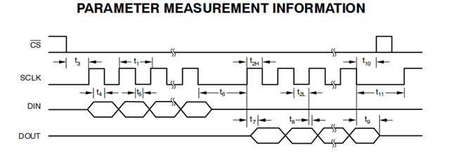
I have attached the wave form showing SCLK, CS and MOSI. The timing between SCLK, CS and MOSI meets the timing specification shown below. And the consecutive MOSI bytes also meets timing requirements. The MISO was not shown, but in the test, it always stayed high.
The following figure showed when writing a single byte. Blue line -- CS, Yellow line -- SCLK, Purple line -- MOSI.

The following figure shows when writing multiple bytes. Green line -- CS, Purple line -- SCLK, Blue line -- MOSI

I have also attached the configuration code. This is ADC set up.
// adc_spi.c

#include "adc_spi.h"
#include "DSP28x_Project.h"
#include "spi.h"

enum
{

	REG_STATUS = 0x0000,	// x1H
	REG_MUX    = 0x0100, // 01H
	REG_ADCON  = 0x0200, // 20H
	REG_DRATE  = 0x0300, // F0H
	REG_IO     = 0x0400, // E0H
	REG_OFC0   = 0x0500, // xxH
	REG_OFC1   = 0x0600, // xxH
	REG_OFC2   = 0x0700, // xxH
	REG_FSC0   = 0x0800, // xxH
	REG_FSC1   = 0x0900, // xxH
	REG_FSC2   = 0x0A00, // xxH
};


// Command Table

enum
{
	CMD_WAKEUP  = 0x0000,	// Completes SYNC and Exits Standby Mode 0000  0000 (00h)
	CMD_RDATA   = 0x0100, // Read Data 0000  0001 (01h)
	CMD_RDATAC  = 0x0300, // Read Data Continuously 0000   0011 (03h)
	CMD_SDATAC  = 0x0F00, // Stop Read Data Continuously 0000   1111 (0Fh)
	CMD_RREG    = 0x1000, // Read from REG rrr 0001 rrrr (1xh)
	CMD_WREG    = 0x5000, // Write to REG rrr 0101 rrrr (5xh)
	CMD_SELFCAL = 0xF000, // Offset and Gain Self-Calibration 1111    0000 (F0h)
	CMD_SELFOCAL= 0xF100, // Offset Self-Calibration 1111    0001 (F1h)
	CMD_SELFGCAL= 0xF200, // Gain Self-Calibration 1111    0010 (F2h)
	CMD_SYSOCAL = 0xF300, // System Offset Calibration 1111   0011 (F3h)
	CMD_SYSGCAL = 0xF400, // System Gain Calibration 1111    0100 (F4h)
	CMD_SYNC    = 0xFC00, // Synchronize the A/D Conversion 1111   1100 (FCh)
	CMD_STANDBY = 0xFD00, // Begin Standby Mode 1111   1101 (FDh)
	CMD_RESET   = 0xFE00, // Reset to Power-Up Values 1111   1110 (FEh)
	//CMD_WAKEUP  = 0xFF, // Completes SYNC and Exits Standby Mode (FFh)
};

static void bsp_DelayMS(Uint16 nms);
static void bsp_DelayUS(Uint16 nus);

static void ADS1256_WaitDRDY(void);
static void ADS1256_ResetHard(void);
static void ADS1256_DelaySCLK(void);
static void ADS1256_DelayDATA(void);
static void ADS1256_DelayCS(void);
static void ADS1256_DelaySYNC(void);

static void ADS1256_WriteCmd(Uint16 _cmd);
//static void ADS1256_WriteReg(Uint16 _RegID, Uint16 _RegValue);
//static Uint16 ADS1256_ReadReg(Uint16 _RegID);
static Uint32 ADS1256_ReadData(void);
static void ADS1256_SetChannal(Uint16 _ch);
//static void ADS1256_StopScan(void);

ADS1256_VAR_T g_tADS1256;
static const Uint16 s_tabDataRate[ADS1256_DRATE_MAX] =
{
	0xF000,		// 30K SPS
	0xE000,		// 15K
	0xD000,		// 7.5K
	0xC000,		// 3750
	0xB000,		// 2000
	0xA100,		// 1000
	0x9200,		// 500
	0x8200,		// 100
	0x7200,		// 60
	0x6300,		// 50
	0x5300,		// 30
	0x4300,		// 25
	0x3300,		// 15
	0x2300,		// 10
	0x1300,		// 5
	0x0300		// 2.5
};


void bsp_DelayUS(Uint16 nus)
{
	DELAY_US(nus);
}


void ADS1256_Init(){
    EALLOW;

	// CS
	GpioCtrlRegs.GPAMUX1.bit.GPIO6=0; // GPIO
    GpioCtrlRegs.GPAPUD.bit.GPIO6=0; // Enable internal pullup
    GpioCtrlRegs.GPADIR.bit.GPIO6=1; // Output

	//RST
    GpioCtrlRegs.GPAMUX1.bit.GPIO7=0; // GPIO
    GpioCtrlRegs.GPAPUD.bit.GPIO7=0; // Enable internal pullup
    GpioCtrlRegs.GPADIR.bit.GPIO7=1; // Output

	//SYNC
    GpioCtrlRegs.GPAMUX1.bit.GPIO8=0; // GPIO
    GpioCtrlRegs.GPAPUD.bit.GPIO8=0;  // Enable internal pullup
    GpioCtrlRegs.GPADIR.bit.GPIO8=1;  // Output

	//DATA READY
	SysCtrlRegs.PCLKCR3.bit.GPIOINENCLK = 1; // GPIO input clock
    GpioCtrlRegs.GPAMUX1.bit.GPIO9=0; // GPIO
    GpioCtrlRegs.GPAPUD.bit.GPIO9=1;  // Disable internal pullup
    GpioCtrlRegs.GPADIR.bit.GPIO9=0;  // Input
	GpioCtrlRegs.GPAQSEL1.bit.GPIO9= 0;


	GpioDataRegs.GPASET.bit.GPIO6=1; // Set value
    GpioDataRegs.GPASET.bit.GPIO7=1; // Set value
    GpioDataRegs.GPASET.bit.GPIO8=1; // Set value


	EDIS;
};

// t11 -> min 1/7.68M * 4 = 0.52 us Delay for final SCLK falling edge to first
// rising edge of next command, WREG, RREG, RDATA
// RESET and SYNC must be low for at least 0.52 us to be effective
static void ADS1256_DelaySCLK(void)
{
	bsp_DelayUS(1);
}

// t11 -> min 1/7.68M * 24 = 3.12 us Delay for final SCLK falling edge to first
// rising edge of next command, RDATAC, SYNC

static void ADS1256_DelaySYNC(void)
{
	bsp_DelayUS(5);
}

// t8 -> min 1/7.68M * 8 = 1.04 us Delay for final SCLK falling edge to first
// CS goes high

static void ADS1256_DelayCS(void)
{
	bsp_DelayUS(3);
}

// t6 -> min  50 * 0.13uS = 6.5uS
// Delay from last SCLK edge for DIN to first SCLK rising edge for
// DOUT: RDATA, RDATAC,RREG Commands

static void ADS1256_DelayDATA(void)
{
	bsp_DelayUS(10);
}

// SCLK period 37.5 M / 60 = 625K
// 1/625k = 1.6 us

// Data ready time

static void ADS1256_WaitDRDY(void)
{
	Uint32 i;

	for (i = 0; i < 40000000; i++)
	{
		if (DRDY_IS_LOW())
		{
			break;
		}
	}
}

// Write register

void ADS1256_WriteReg(Uint16 _RegID, Uint16 _RegValue)
{
	ADS1256_WaitDRDY();

	spi_xmit(CMD_WREG | _RegID);

	DELAY_US(10);
	ADS1256_WaitDRDY();
	spi_xmit(0x0000);

	DELAY_US(10);
	ADS1256_WaitDRDY();
	spi_xmit(_RegValue);

}

// Send command

static void ADS1256_WriteCmd(Uint16 _cmd)
{

	DELAY_US(10);
	spi_xmit(_cmd);
	DELAY_US(10);

}


void ADS1256_CfgADC(ADS1256_GAIN_E _gain, ADS1256_DRATE_E _drate)
{
	g_tADS1256.Gain = _gain;
	g_tADS1256.DataRate = _drate;

	ADS1256_StopScan();

	ADS1256_ResetHard();

 	ADS1256_WriteCmd(CMD_RESET);
 	DELAY_US(60);
 	ADS1256_WriteCmd(CMD_SDATAC);
 	DELAY_US(60);

	{
		Uint16 buf[4];
		buf[0] = (((0 << 3) | (1 << 2) | (0 << 1))<<8);
		// write 00000100, MSB, auto-calibration, buffer disable
		buf[1] = 0x0800;
		// output mux 00001000
		buf[2] = (((0 << 5) | (0 << 3) | (_gain << 0))<<8);
		// no clock out, sensor detect off, gain 1
		buf[3] = s_tabDataRate[_drate];

		//ADS1256_DelaySCLK();
		DELAY_US(20);
		spi_xmit(CMD_WREG | 0);

		DELAY_US(20);
		spi_xmit(0x0303);

		DELAY_US(20);
		spi_xmit(buf[0]);

		DELAY_US(20);
		spi_xmit(buf[1]);

		DELAY_US(20);
		spi_xmit(buf[2]);
        DELAY_US(20);

		spi_xmit(buf[3]);
		DELAY_US(20);
	}


	DELAY_US(50);

	ADS1256_WriteCmd(CMD_SYNC);
	DELAY_US(20);
	ADS1256_WriteCmd(CMD_WAKEUP);
	DELAY_US(800);

}


static void ADS1256_ResetHard(void)
{
	RST(0);
	DELAY_US(10);
	RST(1);

	SYNC(0);
	bsp_DelayUS(2);
	DELAY_US(10);
	SYNC(1);
	DELAY_US(800);

	ADS1256_WaitDRDY();	/* Ready time 630us */
}

Uint16 ADS1256_ReadReg(Uint16 _RegID)
{
	Uint16 read;
	read = 0;
	ADS1256_WaitDRDY();

	DELAY_US(20);
	spi_xmit(CMD_RREG | _RegID);
	DELAY_US(20);
	spi_xmit(0x0000);

	DELAY_US(20);
	spi_xmit(0xEEEE);

	read = SpiaRegs.SPIRXBUF;

	DELAY_US(10);


	return read;
}

Uint16 ADS1256_ReadChipID(void)
{
	Uint16 id;

	id = ADS1256_ReadReg(REG_STATUS);

	return (id >> 4);
}
This is SPI set up.
#include "spi.h"
#include "SCI.h"
#include "adc.h"

//SPI send out data
void spi_xmit(Uint16 a){
	SpiaRegs.SPISTS.bit.INT_FLAG = 1;
    SpiaRegs.SPITXBUF = a;
    while(!SpiaRegs.SPISTS.bit.INT_FLAG){}
    //DELAY_US(20);
}

void spi_init(){
    // Initialize spigpio:16--SIMO, 17--SOMI, 18--CLK, 19--STEA

    EALLOW;

    GpioCtrlRegs.GPAPUD.bit.GPIO16 = 0;   //Enable pull-up on GPIO16 (SPISIMOA)
    GpioCtrlRegs.GPAPUD.bit.GPIO17 = 0;   //Enable pull-up on GPIO17 (SPISOMIA)
    GpioCtrlRegs.GPAPUD.bit.GPIO18 = 0;   //Enable pull-up on GPIO18 (SPICLKA)
    GpioCtrlRegs.GPAPUD.bit.GPIO19 = 0;   //Enable pull-up on GPIO19 (SPISTEA)

    //
    // Set qualification for selected pins to asynch only
    // This will select asynch (no qualification) for the selected pins.
    // Comment out other unwanted lines.
    //
    GpioCtrlRegs.GPAQSEL2.bit.GPIO16 = 3; // Asynch input GPIO16 (SPISIMOA)
    GpioCtrlRegs.GPAQSEL2.bit.GPIO17 = 3; // Asynch input GPIO17 (SPISOMIA)
    GpioCtrlRegs.GPAQSEL2.bit.GPIO18 = 3; // Asynch input GPIO18 (SPICLKA)
    GpioCtrlRegs.GPAQSEL2.bit.GPIO19 = 3; // Asynch input GPIO19 (SPISTEA)

    //
    // Configure SPI-A pins using GPIO regs
    // This specifies which of the possible GPIO pins will be SPI
    // functional pins.
    // Comment out other unwanted lines.
    //
    GpioCtrlRegs.GPAMUX2.bit.GPIO16 = 1; // Configure GPIO16 as SPISIMOA
    GpioCtrlRegs.GPAMUX2.bit.GPIO17 = 1; // Configure GPIO17 as SPISOMIA
    GpioCtrlRegs.GPAMUX2.bit.GPIO18 = 1; // Configure GPIO18 as SPICLKA
    GpioCtrlRegs.GPAMUX2.bit.GPIO19 = 1; // Configure GPIO19 as SPISTEA

    EDIS;


	SpiaRegs.SPICCR.all = 0x0008;  // Reset SPI, send out on rising edge, receive on falling edge, 8 bit

    SpiaRegs.SPICTL.all = 0x0006;   //no phase delay master mode

    SpiaRegs.SPIBRR = 0x001D;   // SPICLK(SPICLK 37.5M/(29+1))

    SpiaRegs.SPIPRI.bit.FREE = 1;   // Free run
    //SPI FIFO
    SpiaRegs.SPIFFTX.all = 0xE040;  //enable SPI TX interrupt

	SpiaRegs.SPICCR.all= 0x0088; // Renable SPI

}

interrupt void spi_rx_isr(void){

    SpiaRegs.SPIFFRX.bit.RXFFINTCLR = 1; //Clear inerrupt
    PieCtrlRegs.PIEACK.bit.ACK6 = 1; //
}

interrupt void spi_tx_isr(void){
    SpiaRegs.SPIFFTX.bit.TXFFINTCLR = 1; // Clear interrupt
    PieCtrlRegs.PIEACK.bit.ACK6 = 1; //
}
Look forward for your help.
Thanks
Chad


