This thread has been locked.

If you have a related question, please click the "Ask a related question" button in the top right corner. The newly created question will be automatically linked to this question.

TLC3541: part failure

Part Number: TLC3541

We have been experiencing failures of the TLC3541ID ADC in 15% of our boards. The parameters of the design are; REF=5V, VDD =5.2V, FS is tied to VDD, AIN can be a maximum of 5.3V. Test engineers have stated that the device fails immediately and they can't retrieve good data from the SPI interface. They have mentioned that SDA actually mirrors SCLK after the failure. We have noticed that the CS line comes up before VDD has reached a steady 5.2V. Could that be an issue?

Thanks for any input. 

  • Hi Matthew,

    Welcome to our e2e forum!  Your VDD, VREF and FS tied high all sound fine for the TLC3541.  When you say the devices 'fail immediately' are they actually broken (blown up, never to work again) or you are just not getting the expected data output?  If you can provide a schematic showing the area around the ADC along with some scope captures of /CS, SCLK and SDO - that would be great!

  • Hi Tom,

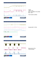
    Thanks for the reply! The test Engineers described the failure as unexpected data output. They claimed that they even saw the SCLK mirrored onto SDO . Once they experience this failure they can't get the part to work correctly again. I asked if they experienced the part getting too hot and they said it wasn't anything like that. I've added some images of the schematic. I hope you can read them easily. I didn't see a way to attach them so i had to insert them in the message body. The first is the ADC and it's reference. The second is the supply for the ADC. The third pic is the buffered analog signal. The fourth picture is the scope output of the supply voltage and the CS signal. I can ask them for some more oscope data. They're overseas and have other priorities so it could take some time. Thanks again!

  • Hi Matthew,

    Thank you for the captures!  The reference and power look fine.  Generally speaking, we recommend an 'RC' ahead of the ADC input, but that should not be the cause of the issue you are seeing.  With the control signals, I would like to see the device initialization/RESET routine from power up as described on page 11 of the datasheet.  Can you provide that for me?

  • Hi Tom,

    Sorry for the late reply. I received the initialization data from the test engineers. It looks correct to me. What do you think? 


  • Thank you Matthew,

    The microcontroller SPI interface should be programmed for CPOL = 0 (serial clock inactive low) and CPHA = 1 (data is valid on the falling edge of serial clock).  I can see that you have CPOL = 1 starting with the initialization and then continuing through the conversion cycles.  It seems as though you are getting some conversion results (SDO does not appear to mimic SCLK), but I can't tell if the conversion results are correct with the resolution of the screen shots and not knowing what your analog input voltage is.  Please set the serial clock to be inactive low and see if that fixes all remaining issues.