This thread has been locked.

If you have a related question, please click the "Ask a related question" button in the top right corner. The newly created question will be automatically linked to this question.

ADC3664: Default output format and wire configuration

Part Number: ADC3664

It seems like the default output format is 14-bits in 2s complement and the DDC is bypassed. I can't quite figure out the default configuration for the number of lanes used. I'm trying to understand if my desired application can work without any SPI configuration or not.

What is the default output format, number of lanes used, FCLK, serialization, etc?

This would be nice to make explicitly clear in the datasheet. 

  • Hello,

    By default, the ADC3664 will be programmed (upon completion of start up time) in the following configuration:

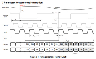
    2-wire, 14 bits, 2s Complement, DDC bypassed, FCLK (0xFFC00, toggles high/low for each frame of data). In 2-Wire/Bypass mode, the serialization rate is 7x. So, if a 125 MHz sample clock is used, then the DCLKIN frequency is 437.5 MHz (SLVDS is DDR, so actually 875 Mbps per wire/lane).

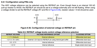
    Another thing to consider, if you do not intend to use SPI interface, is using the REFBUF pin to select the voltage reference (Internal or External) and clocking input (SE or Differential).

    Best Regards,

    Dan