This thread has been locked.

If you have a related question, please click the "Ask a related question" button in the top right corner. The newly created question will be automatically linked to this question.

ADS9120: ADS9120

Part Number: ADS9120

I still have a problem capturing the Converted ADC data out.
To avoid confusion, I do not write to any control register. Staying on SPI-00-S mode (instead of SPI-01 or 11 modes.)
Upon power-up, firmware goes into an endless loop or reading the ADC IC. Everything looks OK going to the ADC IC.

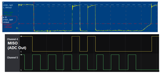
However, Data out is a fixed pattern with pulses being 1/2 the Clock Cycle.

Any ideas or suggestions for me to try? Please see the details, below.
_____________________________________________________________________

With the endless ADC bursts, I see the below for SPI-1 (RF #1-I). MOSI is inactive, always high. ADC output
is not shorted to Clock, yet its bits are not a full clock cycle. The top picture is a scope capture, to rule out
Voltage threshold issues with SPI analyzer looking for 0’s and 1’s.
Supply voltages at ADC IC’s C70 & C77 are 1.9v.  (OK)
RST_L @ R75 is 1.9v.  (OK)
SPI Clock at the ADC IC is 1.9v & 1 uSec. (OK)

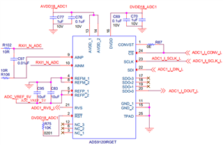
The IC is connected in a standard way.
  • Hi Ramin,

    Is it possible for you to provide a capture of all of the clock and data lines with a logic analyzer so we can verify the format and timing requirements are met?

    Best,

    Zak

  • I provided the CLock and Data Out and Schematics. Due to board density and working remote soldering too many leads is challenging.

    For now, I think I have a RESET issue to correct, which can be the cause. Looking at the Schematics, below are the issues. I welcome your comment on each item.

    1) RSTn is tied to Digital 1.8V supply.
         Q) That does not guarantee IC being ready for rest to be de-asserted?

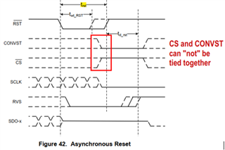
    2) CONVST and CSn are tied together, and never satisfy ADS9120's RESET Exit condition.

        Below is the text from datasheet:

    • To exit RST state, the host controller must pull the RST pin high with CONVST and SCLK held low and CS held high, as shown in Figure 42. After a delay of td_rst, the device enters ACQ state and the RVS pin goes high.

    QUESTION: 
         If CS and CONST are tied together and HIGH with no clock when ADS9120 powers up with its RSTn tied to the power,
         what can be expected of the ADC IC's behavior? Unpredictable? ...

  • Hi Ramin,

    Holding CONVST low when pulling RST high is not a hard requirement. In the case of a single control line for both /CS and CONVST, you can keep both signals HIGH, with SCLK low, when RST is pulled high and still get a full reset of the device. SCLK does still need to be low though to exit reset. I believe it's okay to tie reset high if you do not plan to use it, but it is always best to hold reset low until the supply voltages have stabilized if you are able to do so as this will guarantee a clean startup.

    What is the state of the RVS pin once you pull CS and CONVST high? Do you have an input signal present during the test?

    Best,

    Zak