Part Number: ADS1115
I struggle getting the result I expected from ADC. I have checked everything again and again believing I did something wrong in the protocol but everything should be correct to data sheet. Here is what is happening :
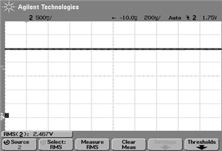
- ADC value seems only to have 12 bits as last 4 bits always are zero
- Even I set ²2.048 Volt VREF it seems is is only 25% in reality
- Regardless of MUX settings I seem to read AIN0 (+) and GND (-) (Setup is AIN0 (+) and AIN3 (-)
- AIN1/AIN3 and AIN2/AIN3 reads similar as AIN0/AIN3
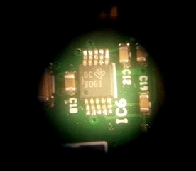
The chip I have is marked "BOGI" as order code "ADS1115IDGSR" says but still it appears that this in reality is a different ADC. I found others having the same problem with this device.
https://forum.arduino.cc/t/ads1115-problems-or-fake/658746
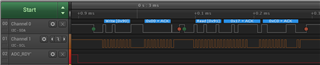
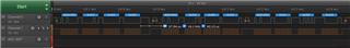
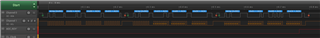
Init and start ADC:
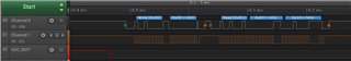
Read ADC:
BR
Morten