This thread has been locked.

If you have a related question, please click the "Ask a related question" button in the top right corner. The newly created question will be automatically linked to this question.

DAC5311: DAC output ringing

Part Number: DAC5311

Dear Expert

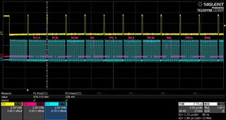
1. Ch 1 CS Pin ,Ch2 Clock ,Ch3 Input

2. Ch 1 CS Pin ,Ch2 Clock ,Ch3 output

3.Bode diagram

4. Schemetic

Now we have question is this chip, input normal, output have two problems, one is jitter, the other is in the way of rising, output concave .

Could u give some suggestion about our desgin ?

  • Hi Gabriel,

    Can you clarify what input and output you are referring to in the oscilloscope shots? Is it the DAC input and output? Op amp input and output? Can you also send a zoomed in oscilloscope shot of the issue you are seeing so we can see the output behavior?

    Thank you,

    Katlynne Jones

  • Hi Katlynne,

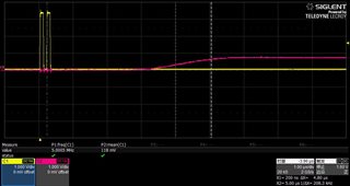
    The first video above is  from  DAC5311 pin 1 2 6  which meas the nsync  clk  vout of DAC5311. 

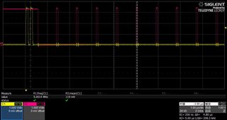
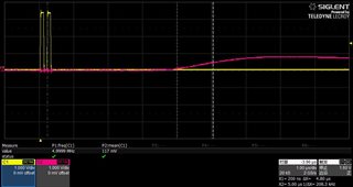
    The second video above is from  DAC5311 pin 1 2 3 which meas the nsync  clk  din of DAC5311.

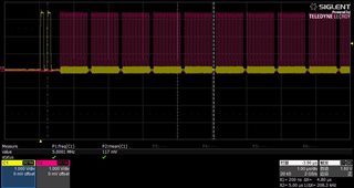
    1-sync(yellow)  2-clk(blue)  3-din(red)

    The third picture is the data which the controller write to DAC5311, you can see the data is increasing  without  decrease. However from the first video  we can see the output concave at the beginning.

    What's more, the din is very stable but the output is jitter in the first video.

    The picture below is the nSYNC  CLK  DIN  VOUT to Pulser. 

    A///1-Pulser(yellow) 2-nSYNC(red)

    1-Pulser(yellow) 2-nSYNC(red)

    B///1-Pulser(yellow) 2-clk(red)

    1-Pulser(yellow) 2-clk(red)

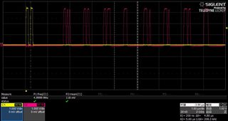
    C///1-Pulser(yellow) 2-DIN(red)

    C///1-Pulser(yellow) 2-DIN(red)

    D///1-Pulser(yellow) 2-VOUT1(red)

    D///1-Pulser(yellow) 2-VOUT1(red)

    E///1-Pulser(yellow) 2-VOUT2(red)

    E///1-Pulser(yellow) 2-VOUT2(red)

  • Hi Aaron,

    Thank you for clarifying!

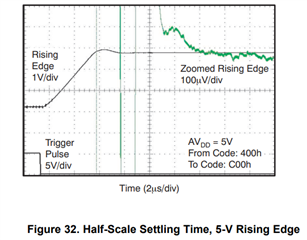
    The concave behavior you see at the beginning of the DAC output comes from the settling of the DAC output buffer.

    You can see similar behavior in this typical characteristics table from the datasheet:

    AVDD is used as the reference for the DAC5311. Can you measure the AVDD supply to see if the jitter is present there as well?

    Thank you,

    Katlynne Jones

  • Hi Katlynne,

    Thank you for your reply.

    The concave we see from picture 1, is the same as the figure 32 from the datasheet. Well, that's ok as this's not the key point.

    But the jitter is the fatal flaw in our design. This will change the time sequence of some signals.

    We used a battery which is 3.7V as the power supply AVDD of DAC5311, but the jitter is present as well.

    And we also used a linear DC power supply to AVDD, it's the same.

    Oherwise, the jitter will be gone when we changed another DAC5311. We have 10  boards  which are in the same batch. There are 4 board having the jitter. We changed 2 DAC5311, the jitter is gone.

    Our another project also use DAC5311,  there is no jitter and the design is the same.

    • Most DACs will see a longer delay when slewing from code 0x000. I think in the picture you showed, you are starting at 0 volts. Can you do this test again, but use code 8 as the minimum voltage?

    Thanks

    Paul

  • Hi Paul,

    The jitter is gone when we use code 8 as the minimum voltage.

    Great. So what's the reason?

    Thanks,

    Arron

  • Hi Arron,

    When the DAC is set to code 0, the output buffer is at the negative rail (GND) and it takes extra time to exit this condition. The same is true when the DAC is at full scale and is at the positive rail (VDD). Code 8 was likely to work in the test Paul suggested, but you can try with codes smaller than 8 as well.

    Best,

    Katlynne Jones 

  • Hi Katlynne Jones,

    Thank you for your advice. 8 is ok for  our  system. Now the problem is over.

    Also thank Paul for helping.