This thread has been locked.

If you have a related question, please click the "Ask a related question" button in the top right corner. The newly created question will be automatically linked to this question.

AFE5809EVM: setting Down conversion frequency, CW outputs (J12, J13), Register Direct Access tab (In AFE5809GUI), CW summing amplifier

Part Number: AFE5809EVM
Other Parts Discussed in Thread: AFE5809

Hi Mr/Miss,

May I clarify the following questions that I have with regards to the AFE5809EVM and its corresponding GUI:

1. I understand that based on the AFE5809 datasheet, the down conversion frequency equation is given as "f = (N*Fs)/(2^16)", where Fs = ADC sampling frequency. Just to be sure, may I confirm that the value of N of that equation is set by assigning a value to the register "MANUAL_FREQ" in the AFE5809GUI?

2. May I also confirm that the CW outputs J12 and J13 will only display the waves of I and Q channels in CW mode, and as such, when the settings of components in the TGC/Pulsed-wave imaging mode, say the Demodulator, for instance, are changed, they will not be reflected in the CW outputs J12 and J13 because they are dedicated outputs for the CW mode/path only?

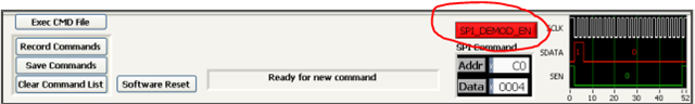
3. May I also ask with regards to the Registers Direct Access Tab in the AFE5809GUI, more specifically the Readout_Mode, how exactly do we use it?
For example, If I were to enable Readout_Mode and read the address 0x21, will the bits [15:0] of the Data that I receive be the value of MANUAL_FREQ?

4. May I check with regards to the CW mode I/Q channel outputs from J12 and J13, if I were to apply an input CW analog signal to CH 1 and i only want to view CH 1's I/Q CW output instead of the summed outputs, is the only way to achieve this is to ground the remaining 7 channels? Or will disabling the "CW_SUM_AMP_ENABLE" register in the "Register Direct Access" tab of the AFE5809 GUI achieve the same effect as well?

Thank you very much for your help and stay safe!

Ps: I have read the AFE5809 datasheet and AFE5809EVM guide and I sincerely apologise if any of the answers to the rudimentary questions asked above can be found in the datasheet as this is my first time using an EVM and I am trying to check back on my understanding based on what I have understood from the datasheets.

  • Hi Jovin,

    Please find my response to your queries below,

    1) Yes. MANUAL_FREQ field in the GUI sets the N value in the device through which down-conversion frequency is computed.

    2) CW mode outputs are not sensitive to TGC settings like, VCA gain, PGA gain and any ADC related settings. You may also note that device can either support TGC mode or CW mode but not both the modes at the same time.

    3) You can write the device registers directly via Register Direct access tab. You can also read back the already configured register using this tab. While using it please ensure that whenever demodulator registers are being accessed, SPI_DEMOD_EN is set as shown below,

    4) If CW Summing amplifier is disabled, the CW outputs will won't swing at all. They'll be grounded. Summing amplifier is very crucial for CW operation. If you want only CH1 input in the CW output, as you suggested you can give signal to CH1 and ground all the other channels.

    Hope I answered all your questions. Kindly let us know for further queries.

    Regards,

    Kalyan

  • Hi Kalyan,

    Thank you for your reply, I appreciate your help! With regards to your reply to question 3, I did some a simple test on my AFE5809EVM to read Register Address 0xC0 and obtain the value of bit [1], which is the demodulator register "REGISTER_READOUT_ENABLE".

    The steps below was what I have done in detail:

    1. Powered up AFE5809EVM and connect it to my laptop without changing any of the GUI settings

    2. In Register Direct Access Tab -> Set SPI_DEMOD_EN as you have advised

    4. In Register Direct Access Tab -> Configure Readout_Mode to "Enabled"

    3. Proceeded to read Register Address 0xC0 to find out the value of bit [1], which is the REGISTER_READOUT_ENABLE bit


    However, i obtained a data value of 0x0, which is incorrect as bit[1] should have been set as 1 when register readout mode has been enabled.

    I expected to read a value of 0x2 instead, which was not the case... I have attached a screenshot of what i have just described below.


    Side Note: Additionally, there have been several cases where I have read other demodulation registers but i only got "0xFFFF" as the Data, which should not be the case as based on my limited understanding of the AFE5809 datasheet, most of the unused registers are set as 0 by default during the AFE5809EVM startup.

    Can you advise on what I have done wrong in trying to read the REGISTER_READOUT_ENABLE bit?

    Because I have tried this multiple times but I still obtained the same result.

    Thank you very much!

  • Hi Jovin,

    Can you please try below suggested sequence and let us know if it worked-

    1. Powered up AFE5809EVM and load any demodulator configuration file/write some demodulator settings.

    2. In Register Direct Access Tab -> Disable SPI_DEMOD_EN bit

    3. In Register Direct Access Tab -> Configure Readout_Mode to "Enabled"

    4. In Register Direct Access Tab -> Set SPI_DEMOD_EN bit

    5. Try to read any demodulator setting related register. Please try to avoid reading register which have REGISTER_READOUT_ENABLE bit. If you have programmed setting like decimation factor before starting read sequence, that register can be read.

    Regards,

    Kalyan