This thread has been locked.

If you have a related question, please click the "Ask a related question" button in the top right corner. The newly created question will be automatically linked to this question.

ADS4149EVM: I'm not good at using the ADC, so I'd like to ask you about the approximate usage.

Part Number: ADS4149EVM
Other Parts Discussed in Thread: ADS4149

Hello.

I'll measure the analog output  of the CMOS IC chip using the ADS4149EVM. I'm not good at using the equipment, so I'm asking you the following question.

1) When connecting through TSW1400EVM and ADS4149EVM LVDS terminals, should both the Capture Board and ADC be connected to USB? Also, do I have to apply a clock to both ADC and Capture Board?

2) I wonder which elements should be soldered to measure differential signals through the ADC equipment. Also, I don't know which terminal needs soldering.

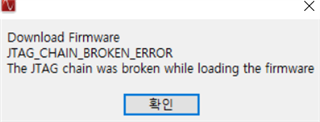
3) We tried to conduct a simple test by connecting the TSW1400EVM combined with the ADC to the computer through USB, turning on the HSDC, and applying a Square wave to the IN+, but such an error occurs.
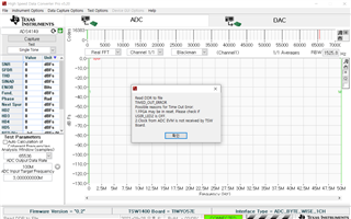

Additionally, I'm giving you some additional photos of the setting status. I would appreciate it if you could let me know what additional problems are.

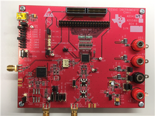
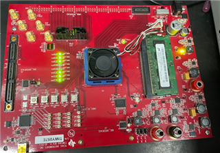
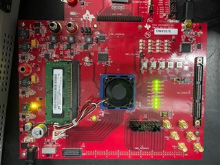
The pictures below are ADC and Capture Board photos under the same conditions as 3).

1) ADS4149EVM

2) TSW1400EVM
  • Minjae,

    1) When connecting through TSW1400EVM and ADS4149EVM LVDS terminals, should both the Capture Board and ADC be connected to USB? Also, do I have to apply a clock to both ADC and Capture Board? Both boards need a USB connection as they both have GUI's to control them. The ADS4149EVM can be configured to operate without the GUI (parallel).See the ADS4149EVM User's Guide for more info on how to configure this EVM. Only the ADS4149EVM needs a clock input. Again, see the User's Guide for more info.

    2) I wonder which elements should be soldered to measure differential signals through the ADC equipment. Also, I don't know which terminal needs soldering. If you want to inject a differential input, you must remove R84, T1 and T2 and apply a short across pins 3-4 and 1-6 of T1 and T2. You will need to add a 0 Ohm resistor to R82. 

    3) We tried to conduct a simple test by connecting the TSW1400EVM combined with the ADC to the computer through USB, turning on the HSDC, and applying a Square wave to the IN+, but such an error occurs. You probably did not have a clock source connected to the ADS4149EVM and the board may have not been configured properly.

    Regards,

    Jim

    User's Guide.pdf

  • Hello. Jim

    Thank you for your answer.

    As you said, I applied the input clock to the ADC at 1.5Vpp, 3MHz, and connected to the computer for both TSW1400 and ADC to proceed with the test again.

    I turned off Low Latency Mode in GUI, turned Gain on, entered Gain value as 1 dB, and turned HSDC on to press Capture, but the same error occurred. (JP12 pin's Series and Parallel mode were both carried out by moving jumper lines, but the results were not the same.)

    In the Default Jumper Setting state, Section 3.2 in the User Guide and ADC GUI Setting were also applied, but LEDs 3 and 4 of the TSW1400EVM are still off and cannot be measured due to the same error related to the DDR.

    • Move jumper JP12 to short positions 2–3, which places the ADC in serial operation mode.
    • Move jumper JP11 to short positions 2–3, which allows the USB circuit to control SDATA.
    • Move jumper JP9 to short positions 2–3, which allows the USB circuit to control SEN.

    I'm not sure what the problem is.

    +) When 3.3V is applied to the ADC, it consumes about 550 mA.

  • Minjae,

    Per the data sheet, the minimum clock rate is 20MHz for the ADS4149. Please increase your clock rate. Make sure the 5V supply connected to the TSW1400EVM can provide at least 3A of current.

    Regards,

    Jim 

  • Hello. Jim

    Thank you for your answer.

    I forgot to include it in the post, but I changed Input CLK to 50 MHz, but the same error still occurs.

    In addition, it seems that the TSW1400EVM is normally powered through a DC adapter.

    I haven't figured out what the problem is yet. Please let me know if there are any additional problems.

    +)

    Now I understand why you said that after looking at the link below.

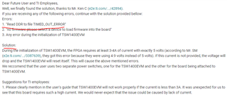
    e2e.ti.https:/.../tsw1400evm-afe5809evm-tsw1400evm-error-read-ddr-to-file-timed_out_error

    Currently, in order to apply 5 V, I want to supply power through Power Supply rather than DC adapter, but I wonder how to do it.

    (For now, Power was applied to 3.3V (J10) only without using 5V adapter after looking at the Guide PDF, but too little current flows to about 100 mA.)

    In addition, when power was applied via adapter for 5V and Power Supply for 3.3V, errors related to the same DDR occurred and no current was applied from the 3.3V terminal. When the ADC Firmware is loaded through USB using only 3.3V terminal, the following error occurs.

  • J10 should only be used as an output 3.3V power source when 5V is connected to J12. Never provide a voltage to J10 as you may damage the board.

    The purpose of J10 is to provide a 3.3V source to the ADC EVM as an option. You need to provide 5V to J12 and verify the 3.3V regulator U12 is still working properly. You should see 3.3V on test point 21. If not, you probably damaged the board.

    The jumpers on the ADC board should match the ones shown in the attached figure.


  • Hello. Jim

    Thank you for your answer.

    The reason I tried that is because I saw the post of the forum. We will avoid such attempts in the future.

    How should I check whether 3.3V regulator U12 is operating normally?

    Although the jumper on the ADC board matches the attached picture, a DDR error occurs in the TSW1400EVM.

    In that case, where is the problem?

    P.S) If you don't mind, can you also show me the board picture of TSW1400EVM?

  • Apply 5V to J12. Do not plug in the ADC EVM.

    Connect to the TSW1400 with HSDC Pro GUI. 

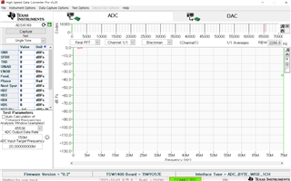
    Select the ADS4149 ini file and download firmware. When this completes, the GUI should look like the screen shot attached.

    There should be 6 status LED's on now. This is a sign the board is working. If you get any message, either the power supply cannot provide enough current or the board is damaged.  

    TSW1400.pptx

  • Hello. Jim

    Thank you for your answer.

    As you said, we conducted the test without plug in ADC.

    I checked that there was nothing wrong with the board.
    The LED is also turned on normally with six LEDs.

    Then, I turned off the power of the TSW1400EVM and conducted the test again as you said with the combination of J10 of the ADS4149EVM and J3 of the TSW1400EVM.

    However, there are still errors related to DDR.

    Is there anything else we can do?

    For example, I would appreciate it if you could let me know the order of connecting ADC and Capture board.

    (I've applied power to ADC, connected Input CLK and Analog Input to apply signals, switched on TSW1400EVM, turned on ADS4149EVM GUI, turned on the ADS4149EVM GUI to enter 1 dB value, and turned on HSDC to upload ADC Firmware.)

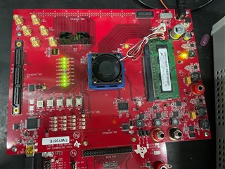
    Add pictures of ADC and Capture Board in case there is something wrong.

    <TSW1400EVM>

    <ADS4149EVM>

    There is a little different part from the ADC picture you sent me.(Blue Circle) Is there an error related to DDR in the TSW1400EVM due to this part?

  • It appears your board is configured for CMOS output not LVDS. Did you make these changes? The board should have shipped with U7 removed and RN3-RN6 installed and R69 and R70 installed. I think this is your main problem. If you board was shipped to you with U7 installed, I would suggest you request for a replacement board.

    If you bought this from a distributor, you will have to work with them to get a replacement. If you bought it from the TI Store, the following link has the details and a link to the form to start the return process.  Once you are on the returns and refunds page of the TI Store look for the hyperlink which says: TI store customer support form. 

    Regards,

    Jim


    www.ti.com/.../ti-store-order.html

  • Hello. Jim

    Thank you for your answer.

    As a result of the discussion, we would like to use ADC through CMOS through an external Logic Analyzer. The picture below is an ADC board picture for CMOS communication.

    Should I set up the jumper pin like this?

  • Set the jumper on J2 to pins 3-4 if you want 2's comp CMOS data or pins 5-6 if you want offset binary CMOS data.