


Other Parts Discussed in Thread: OPA4350, THS4532, THS770006
Dear all,
I have been working on a project that requires reception of four analog data channels using an FPGA. These analog channels have a range of [0.5 : 2.9]V. I need to abide by the following requirements:
OUTPUTS:
- Load impedance of the analog outputs must be equivalent to a resistance of over or equal to 1MOhm.
- Load parasitic capacitance of the analog outputs must be less than 20pF.
ADC:
- Resolution >= 14bits, ENOB >= 13 bits;
- Differential analog input = 2Vpp;
- Fsampling = 25MHz;
- SNR > 74dB;
- THD > 80dB;
- INL < 3LSB
The only ADC that I have found to provide everything (along with 4 channels) is the ADS5263 configured in 14 bit mode. This allows me to interface the ADC with the FPGA using LVDS, which is perfect. However, I'm having troubles designing the ADC driving circuit.
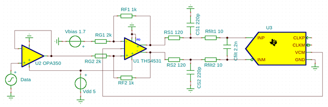
An OPA4350 is used to comply with the high load impedance and low parasitic capacitance requirements. Each channel connects to each opamp in a non-inverting, unitary gain configuration. According to datasheet, the following input impedances apply:
- Differential: 100 TOhm || 2.5 pF
- Common-mode: 100 TOhm || 6.5 pF
Next, since the ADS5263 works best with differential input, two THS4532 are used to convert each channel from single-ended to differential. These FDAs are also used to convert the [0.5 : 2.9]V range into [1 : 2]V required by the ADC in 14bit configuration (2Vpp). Finally, a filter network interfaces each THS4532 output into the ADC.
The resulting schematic for each channel is as below:
My questions are as following:
1. Are the ICs correctly selected, keeping in mind my Fsampling will be fixed at 25MSPs?
2. Should Rf and Rg be of lower value, keeping the same ratio?
3. I cannot for the life of me figure out how to design Rs, Cs and Rfilt for my application. The ADS5263 datasheet suggests using a 5 to 15 Ohm resistance on each analog input (which I have named Rfilt), but I cannot find how to tune the values.
4. Should Cfilt be included seeing this is a DC coupled application?
I'm not at all experienced with analog designs, and if there is any documentation that you feel is relevant I will gladly read it.
Thank you in advance
