This thread has been locked.

If you have a related question, please click the "Ask a related question" button in the top right corner. The newly created question will be automatically linked to this question.

DAC81404 Configuration and Control Through SPI

Other Parts Discussed in Thread: DAC81404, DAC81404EVM

For DAC81404, I managed to use Arduino Uno to configure and control its voltage output.

This is code for DAC setting.

  // Chip Select 
  pinMode(DAC_SS_PIN, OUTPUT);
  digitalWrite(DAC_SS_PIN, HIGH);
    
  // DAC Reset
  pinMode(DAC_RESET_PIN, OUTPUT);
  digitalWrite(DAC_RESET_PIN, HIGH);

  /*** ***
    This delay is very important !!! 
    *** ***/
  delay(100);

  // Write
  write_reg(0x03, 0x04); // SPICONFIG: DEV-PWDWN=0
  write_reg(0x04, 0x0); // GENCONFIG: REF-PWDWN=0
  write_reg(0x09, 0x0); // DACPWDWN: DACx-PWDWN=0, x={A,B,C,D}
  write_reg(0x0A, 0x02); // DACx-RANGE=0b0101, i.e. +/-5V

I used  write_reg(0x10, (i)%65535 ); // DAC-A to adjust channel A's voltage output.

However, when I tried to use an STM32 G431 board, I just cannot make DAC to work.

I have used PicoScope to record SPI wave forms of Uno and STM32 board as follows:

                                                    Uno SPI wave

                                                      G431 SPI wave

If look carefully, G431 signal is better than Uno since for Uno, there are spikes in CS.

For Uno, there is some gap between each byte; however for G431, there is not. Does the gap matter?

  • BTW, the pin connections are as

    EVM board LaunchPad Interface        

       UNO


    3.3v            

      3.3v 

     I found I just need to connect either 3.3 or 5v during 

    5v             

      5v

     configuration. Operation seems not needing those 2

    LDAC         (Left Open)

      6  LDACz_PIN

    Not Set/Reset in Code

    SYNC        

      10  DAC_SS_PIN


    SDIN         

      11  MOSI


    SDO         

      12 MISO

    Not in use; but may need for debugging purpose

    SCLK        

      13 SCLK


    CLR, RST 

       5  DAC_RESET_PIN

     Pull high

  • Hello,

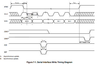
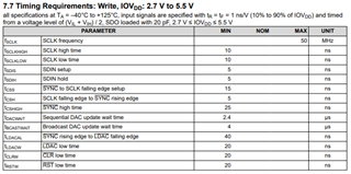
    The SPI frames will need to meet these timing requirements:

    The G431 should work without the gaps that the Uno has as long as the SCLK low and high times are being met. From what I can see in your scope shots, it looks like most of the requirements are being met. Can you zoom in and verify that the SDIN setup and hold times of 5ns before and after each SCLK falling edge are being met? 

    Do you have the correct 3.3V and GND of the G431 connected to the Launchpad interface of the DAC81404EVM? Are the SPI voltage levels of the G431 and Uno both 3.3V?

    You are right that AEVM_5V0 is not used. AEVM_3V3 is used when jumper J19 is closed to use the Launchpad 3.3V as the DAC IOVDD supply. 

    Best,

    Katlynne Jones

  • I just checked that G431 logic high is 3.3v while that of Uno is 5. Could it be the reason? According to data sheet, as long as within range 1.7 to 5v, should be OK.

    In G431 SPI wave, one grid is 5us, in which there are 12 clock pulses. One data bit takes 1 clocks. So within 5us, there are 12 bits, each of which last 417ns. That is more than enough for hold time. For setup time, I need a better scope to double-check.

  • Hello,

    The digital inputs should not be greater than IOVDD. The 3.3V logic level of the G431 should be fine when the IOVDD is connected to AEVM_3V3. When you use the Uno, make sure to connect IOVDD to 5V. 

    Have you been able to write to the DAC using the Uno since trying the G431?

    It looks like you are using the internal reference. When you use the G431, do you see 2.5V on the DAC_VREF node?

    Just to double check, do you have all of the grounds in your system connected? I do not see ground mentioned in the earlier table you shared with the launchpad connections. 

    Best,

    Katlynne Jones

  • Hi Katlynne,

    I managed to make it work, although I still not sure what exactly caused the problem.

    Firstly, the GND pins are connected correctly.

    What I did is using a signal scope to monitor SPI clock, MOSI waves in real time. I found the SPI output mode by G431 was different from Uno, so I adjusted it to the same as Uno.

    Another thing I did: in Uno, I only do configuration ONCE in the setup stage, while in G431 I repeat the same code 10 times during setup. Then subsequently I can change the DAC voltage output as I want.

  • Hi Katlynne,

    I want to read register configuration from the DAC, how many bytes shall I expect from it?

    3 byte, isn't it? 1st one is 0x0, 2nd and 3rd are the setting value.

    My understanding of the data sheet: at SPI MOSI line, I need to send 3 bytes: 1st byte is register address with READ bit set; 2nd and 3rd can be any values. In that period, DAC will send back 2 bytes of values that particular register holds, on SPI MISO line.

  • Hello,

    You should expect 3 bytes:

    The address bits are echoed and then the 16 data bits.

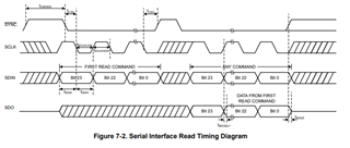
    You need to send a read command, and then a "dummy" cycle to activate the clock so the read back data can be clocked on the MISO line:

    The read command is the register address with read bit as you said. Second and third bytes can be anything. The second "dummy" cycle can be all 0's, or another read or write command.

    Best,

    Katlynne Jones