This thread has been locked.

If you have a related question, please click the "Ask a related question" button in the top right corner. The newly created question will be automatically linked to this question.

ADS8363: ADC Incorrect at low temperature

Part Number: ADS8363
Other Parts Discussed in Thread: OPA2365

Hi 

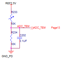
      My circuit is below, R233  is  a NTC thermistors, -10℃ R233 is 275.8Kohm, 25℃ R233 is 50Kohm, 70℃ R233 is 8.663Kohm.

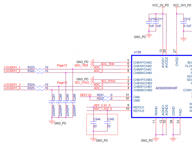
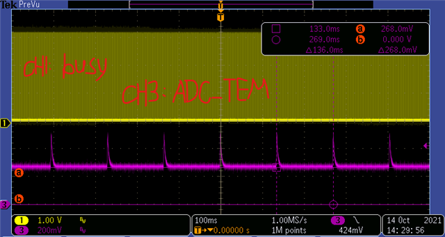
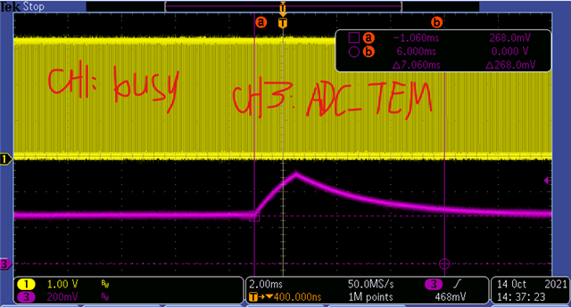
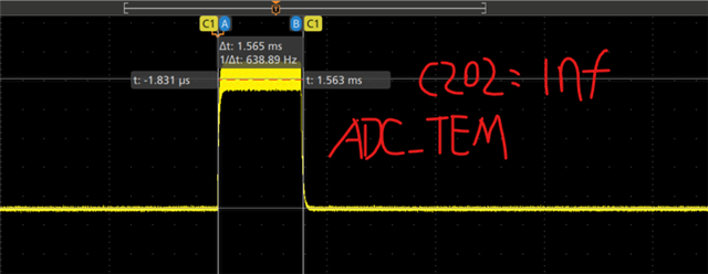
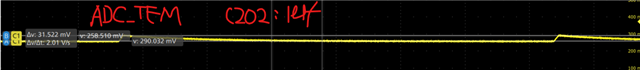
      When I use ADS8363 sample ADC_TEM, when environment temperature lower than 25℃, the ADC result bigger than expected value, when the temperature is lower than 0℃, the ADC result is worse.

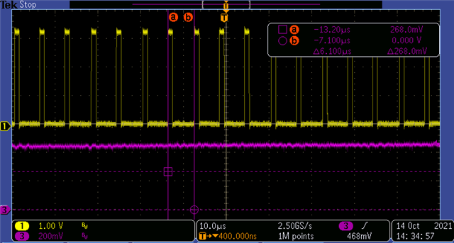
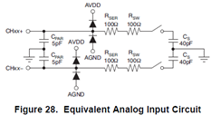
       Test with oscilloscope and found that ADC_TEM has glitches when sampling, sampling interval is 6us. The incorrect ADC result is match with glitches, I guess the glitches is caused by ADS8363 internal sample-and-hold capacitors Cs, when temperature lower, ADC_TEM voltage is lower, Cs will through Rsw, Rser, R233 discharge, then cause ADC_TEM bigger.

       So I has some questions need your help:

1. The incorrect ADC result is caused by Cs precharging?

2. Is a operational amplifier is  necessary for ADS8363 analog input to reduce source impedance? 

3. In datasheet page 19 describe: "After the conversion completes, both capacitors are precharged for the duration of one clock cycle to the voltage present at the REFIOx pin. After precharging, the multiplexer outputs are connected to the sampling capacitors again."  For example, if ADC_TEM continuous sampling 256 times, the Cs will be precharged 256 times? Is it possible to modify the register configuration so that Cs only needs to be precharged once during continuous sampling?

4. How the switch between Cs and Rsw controlled? When  continuous sampling, the switch can always be closed?

Hope your answer, Thanks very much!!!


  • Can someone help me?

  • What is the root cause?

  • Hello Lei,

    Thank you for your post.

    Most SAR ADCs require an external circuit to provide charge to the internal sample-and-hold. At a minimum, this circuit is comprised of a single-ended or differential "charge-bucket" R-C circuit. In your schematic, C202 would serve this purpose and should be placed close to the ADC input. 100 nF is a bit large and may have too much inductance to charge the internal capacitors quickly. You can try reducing this to 1 nF or stacking a small capacitor in parallel.

    A driving amplifier may be required to fully settle the input voltage to less than 1/2 LSB (i.e. below the quantization noise of the ADC). The OPA2365 is one of the recommended amplifiers in Section 9.1.2 of the data sheet.

    Can you provide some examples of the ADC conversion results to show what type of error this is?

    The internal sample-and hold caps are pre-charged at the end of each conversion cycle for a duration of one clock period. Following the pre-charge period is the acquisition period. You can try slowing down your clock to lengthen the acquisition period if the max data rate is not required. This will allow more time for the input voltage to settle in your circuit.

    The input switches open and close with each acquisition period.

    For more information on SAR ADC sampling, please see our TI Precision Labs - ADCs training portal. We cover many of these topics extensively, including sizing the R-C "charge-bucket" and choosing the input drive amplifier.

    Regards,

    Ryan

  • Hi Ryan

        Thank you very much for your help.

        In fact, ADC conversion results is right, it’s just that the result has a big error with my expectations. For example, ambient temperature is -5℃,ADC conversion result is +2℃,  ambient temperature is -10℃,ADC conversion result is -1℃,  the reason I think is acquisition speed is fast, and C202 charged-discharged time too long.

         Due to PCB area limitation, I don't use a amplifier between ADC_TEM and analog input.

          At your suggestion, we modify the  sampling interval from 6us to 200us, ADC conversion result is OK.

          I change C202 from 0.1uF to 10nF or 1nF, ADC_TEM  glitches is bigger, but change c202 to 1uf, the result is good, Is it because the capacitance becomes larger and the charging speed of Cs to C202 becomes slower?


  • Hi Lei,

    A larger capacitor will hold the input voltage more steady, meaning the transient spikes you observe at the beginning of the acquisition period will be smaller. However, the R-C time constant will be much, much slower and the input will never fully settle during the acquisition window. The voltage spike at the beginning of tacq is not the concern. Instead, the important thing is the remaining voltage error at the end of tacq. This is why lengthening the acquisition period to 200 us improved your results.

    Is tacq = 200 us an acceptable solution in your system?

    Regards,

    Ryan

  • Hi Ryan

        Lower acquisition speed is acceptable,  thanks for your help very much!