This thread has been locked.

If you have a related question, please click the "Ask a related question" button in the top right corner. The newly created question will be automatically linked to this question.

Prosthesis using ads1298

Other Parts Discussed in Thread: ADS1298, DRV8412, INA121

Hi,

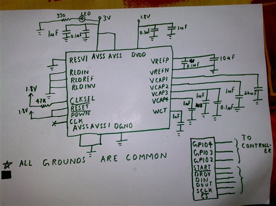
I have undertaken the final year project of myoelectric prosthetic upper limb. It was only a few weeks ago when I found out abou ads1298, so I ordered it immediately.

I am good at At89C51 DIP package and done many projects using it. I have no experience of using an SMT package. I use Proteus Design software for simulating and designing boards. But it has no package for Ads1298. I read the datasheet of ads1298 and learnt that it had an SPI module. I can arrange a usb programmer which uses SPI for programming ATmega16 or ATmega32, but it uses its own computer software. 

Please advise for designing and programming ADS1298 IC.

Eagerly awaiting your reply.

Zahak Jamal

  • Hi Zahak,

    Your ADS1298 project sounds very interesting! For the ADS1298, in either the TQFP or BGA package, there are dimensional drawings in the back of the datasheet that you can use to create your own footprints. There are also footprint/symbols available for the TQFP package for use with Cadence Allegro, as well as Mentor Boardstations and PADS-Power PCB products. However, I don't have any advice with regards to Proteus tool and the ADS1298, since we do not have any experience with that software. You could inquire with those at LabCenter to see if they can help you with a package/symbol.

    From the software side of things, there are several posts in this forum that have timing diagrams of the SPI interface for the ADS1298. The best way to get started is to simply set up your SPI peripheral, so that the SCLK dwells low with data valid on the falling SCLK edge (SPI Mode 1) as noted in the datasheet on page 15 (figure 1). Start off by reading the register defaults,, the device ID bit, etc to verify you can communicate with the device. From there you can try writing to the registers and read them back to ensure everything is working. Let us know how your Prosthetic limb project turns out - maybe you can post us a picture or two when you're done!

    Regards,

    Michael Wheeler

  • Hi,

    Its says in the datasheet that I can connect the ads1298 IC pins of AVDD and DVDD to unipolar supplies. So, what I can do is connect AVDD to a 3V DC supply and DVDD to 1.8V DC supply, while making grounds AVSS and DGND common to drive ADS1298 IC. Am I right?

    Why are there more than one AVSS, AVDD, DVDD and DGND in the IC, as this is not common in other ICs?

    In reference to my previous query. From this IC I only need the PGAs, the ADCs and the GPIO pins. As the IC has no timer or PWM channel hence, I have to connect the output from the GPIO pins to a microcontroller in order to generate PWM. Can I leave the pins like TEST_PACEx, WCT and RLD(and related RLD) pins. 

    I want to thank you for your reply to my previous query, I am now designing the circuit with a similar TQFP package I found in Proteus. Can I use Keil Software or MPlab software for programming the IC in C environment? I have never used MPlab, so I hope your answer is Keil.

    These are basic questions. Its because I have never used such an IC before.

    eagerly awaiting your reply.

     Zahak


  • Hello Zahak,

    "Its says in the datasheet that I can connect the ads1298 IC pins of AVDD and DVDD to unipolar supplies. So, what I can do is connect AVDD to a 3V DC supply and DVDD to 1.8V DC supply, while making grounds AVSS and DGND common to drive ADS1298 IC. Am I right?"

    You are correct. If you look at page 75 figure 73 this is the configuration shown in the example for single-supply operation. The following page of the datasheet also shows an example schematic for using the device with a bipolar supply.

    "Why are there more than one AVSS, AVDD, DVDD and DGND in the IC, as this is not common in other ICs?"

    That's a tough question to answer since I was not the designer of the part. This happens for a variety of reasons; sometimes the layout of the IC just doesn't work out in such a way that you can route all the supply rails to a single pin, sometimes it is to source more current to the IC, and sometimes each pin is supplying different features of the part such that those pins only draw power when certain features are in use to conserve energy.

    "Can I use Keil Software or MPlab software for programming the IC in C environment? I have never used MPlab, so I hope your answer is Keil."

    The answer to this question should be yes to both. It just depends on the microcontroller you are using and if that microcontroller supports those toolchains. The ADS1298 is not really impacted by what IDE you end up using. As long as you can "wiggle" the right lines at the right time on your SPI interface you should be good.

  • Hi Zahak,

    Just to expand on Kevin's remarks:

    "In reference to my previous query. From this IC I only need the PGAs, the ADCs and the GPIO pins. As the IC has no timer or PWM channel hence, I have to connect the output from the GPIO pins to a microcontroller in order to generate PWM. Can I leave the pins like TEST_PACEx, WCT and RLD(and related RLD) pins."

    Typically, output pins do not have to be tied to anything. Same is the case here. However, 'Active Low' type pins should be tied high, and some inputs need to be tied low. In particular:

    /PWDN - Tied high, /RESET - Tied high, RLD INV - Tied GND, RLD REF - GND, RLD IN - GND. Other such inputs may be left open (like the channel inputs not being used, & WCT; although, tying the unused inputs to GND may lower the noise to the ADS1298, this is still not necessary). [You can use Page 21, Figure 23. Functional Block Diagram, of the ADS1298 Datasheet as a reference.]

    Regards,

    Michael

  • Hi,

    Sir, what is the internal reference of the ADCs of ADS1298? It  says in the data sheet that we can use 2.4V for 3V digital supply and 4 for 5V supply as reference. But I can't understand how this works and what will be the resolution of the ADCs?

    I also read in the datasheet that a gain of 6 is enough for an ECG signal. What do you recommend for an EMG signal which ranges between 2 to 20mV @ 30 to 150Hz?

    In reference to my previous post, is my approach correct? i.e taking differential inputs from the INxP and INxN pins, then applying gain on the inputs from the PGAs and then inserting the resulting gain into the ADCs, setting a threshold from the resulting output and then sending a high or low signal to the GPIO pins which go into a microcontroller or directly into a motor driver IC.

    Can it all be possible with the ADS1298 IC?

    Please, I get can get real help from your opinion.

    Just one more basic question, in which registers are the outputs to the ADC stored?

    Also, please recommend an H-bridge or motor driver IC which can be accomodated with the size of the ADS1298 which can give 12 to 24V with 4 or 5A ratings

    Thankyou for your help in the last post.

    Awaiting your reply.

    Zahak Jamal 

  • Why are there more than one AVSS, AVDD, DVDD and DGND in the IC, as this is not common in other ICs?
    Actually, it is common with other ICs. To reduce noise, you need low-impedance power rails, and impedance is made up of resistance and inductance. While you can reduce resistance with thicker wires, inductance is best reduced with multiple wires. The higher speed or more noise-sensitive the chip, the more power and ground pins. Big FPGAs dedicate almost half their pins to power and ground.

    The other rule of thumb is one decoupling capacitor per power pin. Again, for the same reason: lower impedance on the power supply. (You can usually get away with less, but cost-optimize the design later.)

    As for surface-mount, I have no idea why so many hobbyists are so scared of it. All the technicians where I work actively prefer surface-mount components for hand work because they don't need to keep flipping the board over. Not to mention that unsoldering pins is so much easier. The three essential ingredients are a temperature-controlled soldering iron with a variety of tips (particularly chisel tips), liquid flux (if in doubt, add more flux), and copper braid solder wick (which doesn't work for **** until you wet it with flux, then it works great) to pick up excess blobs. A standard hand-soldering technique for fine pitch parts is to solder everything together with a big blob, and then clean off the excess with solder wick.

    BGAs are a pain to do by hand because you need an X-ray machine to see if you did them right.

  • Hi Zahak,

    The internal reference of the ADS1298 is either 2.4V or 4.0V depending on 1.) your analog supply and 2.) the setting of the CONFIG3 register (bit 5).  With an analog supply of 3V as you indicated previously, you would need to use the 2.4V reference option.  The resolution of the ADS1298 is 24-bits.  The LSB weight of the conversion results is VREF/(223-1).  The full scale input range is dependent on the reference voltage and the gain and that's going to be 2VREF/GAIN.  EMG signals are weaker than ECG, so you might need to boost the gain to 8 or 12.

    Taking the EMG signals into the ADS1298 differentially to INxP and INxM is the most common method that I am aware of for EMG measurements.  You are correct with regards to the PGA gain and ADC conversion, but I think you may be off on the GPIO aspect of the part.  The ADS1298 cannot create a PWM signal that would be used to control a micro or motor driver.  Assuming your intention is to read some signals from a muscle and then use that to control a motor (or motors - to move a robotic arm perhaps), you cannot do this with the ADS1298 alone.  The ADS1298 can provide conversion results to a micro which, after post processing, the micro might be able to tell a motor what to do but the ADS1298 does not include any sort of math engine or analysis function to 'intelligently control' its GPIO outputs to that extent.  Your host controller would have to close that loop.

    Take a look at parts like the DRV8412 or DRV8432 for the H bridge driver aspect of this project, these are rated for 12V operation with peak currents to 6A peak in dual bridge mode.

  • Hi,

    Sir, Thankyou, on your previous reply, I think the best way will be of using a microcontroller between the motor drive and GPIO pins of the ADS1298 IC, just as you mentioned.

    I have designed a circuit board of ads1298 using only a unipolar power supply.

    In this case if I give an EMG signal directly, the common mode will lie near 0V, and I won't be able to utilize the IC for the negative values of the signal. 

    For this purpose, can I use an instrumentation amplifier such as INA121 with the REF pin connected to 2.5V so that the common mode range of the output lies in the mid-supply range to ads1298 before inserting the signal to ads1298?

    Please comment.

    Zahak 


  • Hi,

    Sir, I have created a layout of ADS12298 using external unipolar supplies of 3V or 5V (AVDD) and 1.8V (DVDD). The START pin in the schematic is not connected to a controller but can be toggled between DVDD and DGND with the help of a jumper. The pins of GPIO 2-4, /DRDY, /CS, DIN, DOUT and SCLK are to be sent to a microcontroller via a connector. I have designed my layout on Proteus and drew my schematic on a piece of paper, as Proteus doesn't have ADS1298 in a schematic. I am attaching the image of the schematic with this mail. Please, can you verify my schematic.

    Sir, I have no experience of using an SPI module. I know PIC micro to a limited extent. If you can please, send a source code on PIC to write data for suppose setting the VREF_4V bit high(just as an examle) in ADS1298 and retrieve the conversion results of the ADC. As mentioned earlier, I can change START pin high or low with the help of a jumper, so I can also send a START opcode to start ADC conversions while keeping START pin low.

    Where do I connect /DRDY in the micro?

    Can I connect a GPO pin of the micro directly to /CS pin to issue a low signal to activate SPI module of ADS1298? There can also be a voltage difference i.e 5V can be greater than 1.8V(or max DVDD 3.6V). What will I do then?

    anxiously awaiting you reply.

    Zahak 

  • Hi Zahak,

    Your schematic looks ok. But, you have the analog rail tied to 3V (assuming you mean AVdd in your drawing), so setting the reference to 4V would not be applicable. As far as code is concerned, we do not have any code for a PIC microcontroller to offer. DRDY normally gets connected to an interrupt pin on the controller. If your PIC is powered from 5V, you'll need to level shift that down (the SCLK and SDI as well), then possibly level shift up the SDO and DRDY.

    Regards,

    Michael

  • Hi

    I am working on similar project .i.e. Acquisition of multichannel EMG signal for classification of upper limb movements.I am using following components

    ADS1298 IC-For acquiring and digitizing the signals obtained from muscles

    Arduino Uno R3-for configuring the registers and SPI interface with ADS1298

    LabVIEW-acquiring the signal to PC & further processing in LabVIEW software

    As I am new to this IC,I have some questions on interfacing ADS1298 to Arduino board

    1)What are the pin connections between ADS1298 & Arduino board.Is it only the SPI pins(SCK,MISO,MOSI, to be connected? 

    2)As my application is for EMG signal and not ECG/EEG,So I need to configure which all registers(e.g- PGA, /DRDY,/PWDN,/RESET,SPI interface pins)

    Any suggestions on making ADS1298 and Arduino talking serially, will be highly appreciated.

    Thank you

  • Hey Kosha,

    1. Some of the connections to other digital pins will depend on how you  want to use the device. I'd advise that you read the datasheet thoroughly to get a better idea of how to use this device and then if you have any follow-up questions about particular connections, you can follow-up here.
    2. From what I know about EMG, I believe this device is capable of measuring it. The configurations will depend on the specifics of the signal. Do you know exactly the range of amplitudes and frequencies you will have to measure for this application specifically? This will affect how you configure the PGA gain and device data rate.

    Regards,

    Brian Pisani

  • Thank you Brian for quick response.
    The amplitude of EMG signal is in 20 micro-volts to 20 milli-volts range with frequency band of 20-500 Hz. Max PGA for ADS1298 is 12 so is it okay to use ADS1298 as pre-amplifier and how to decide device rate?
  • Kosha,

    From my understanding of EMG, the bandwidth of the signals could extend all the way to 500 Hz. Do you agree? If that is the case, you're going to want to use at least a 2 kSPS data rate.

    Brian
  • Hi Brian,

    I am very much confused about the pin connection of ADS1298 for Multichannel EMG application.
    I have gone through the datasheet over and over again.
    If anyone who already got result with ADS1298 for EMG,can share their experience it will be of great help.

    Thank you
  • Hey Kosha,

    Which pins do you specifically want to understand how to connect? I understand the device functionality well so I can help you with more generic inquiries.

    Regards,
    Brian Pisani