This thread has been locked.

If you have a related question, please click the "Ask a related question" button in the top right corner. The newly created question will be automatically linked to this question.

ADC12DJ3200: Link alarm

Part Number: ADC12DJ3200
Other Parts Discussed in Thread: LMK04828,

Hi,

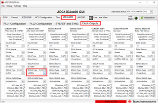
i configured my ADC12DJ3200 as follows:

0x0000 0xB0 // Do soft reset

delay for 100ms
0x0200 0x00 // Clear JESD_EN (always before CAL_EN)
0x0061 0x00 // Clear CAL_EN (always after JESD_EN)
0x0201 0x00 // Set JMODE0
0x0202 0x03 // Set KM1=3 so K=4
0x0204 0x05 // Use TMSTP+/- input, offset binary data, scrambler enabled

0x0205 0x04 // Ramp test mode

0x003B 0x03 // Enable TMSTP Rec and TMSTP LVPECL
0x0213 0x07 // Enable overrange, set overrange holdoff to max period 8*2^7 = 1024 samples
0x0048 0x03 // Set serializer pre-emphasis to 3

0x029 0x30 // enable the SYSREF receiver circuit and Set zoom bit

read 0x02C-0x2E

0x029 0x74 // set SYSREF_PROC_EN and SYSREF_SEL
0x0061 0x01 // Set CAL_EN (always before JESD_EN)
0x0200 0x01 // Set JESD_EN (always after CAL_EN)
0x006C 0x00 // Set CAL_SOFT_TRIG low to reset calibration state machine
0x006C 0x01 // Set CAL_SOFT_TRIG high to enable calibration

After set the master_reset_n signal to ‘1’ and Set the rx_sync_reset_vio signal to ‘0’ in the Reference Design following values are in the Registers 0x0208 and 0x02C1:

0x0208 = 0x0C

0x02C1 = 0x08

So it seems the JESD204 link isn't established

Do you have any advice for me ?

BR

Chris

  • Hi Chris,

    Are you using ADC12DJ3200EVM or this is your own board? If you are using the ADC12DJ3200EVM than you will have to enable the sysref output from the LMK04828 to the ADC. You can enable the SYSREF to the ADC by going to LMK04828->Clock Outputs Tab selecting LVPECL instead of power down. 

    The second thing I noticed is you haven't sysref processing enable in register address 0x29. Without enabling the SYSREF processing the ADC will not look at the SYSREF signal. 

    0x029 0x30 // enable the SYSREF receiver circuit and Set zoom bit

    Please update this line with following:

    0x29 0x70 // enable SYSREF receiver, SYSREF processing and SYSREF zoom.

    Regards,

    Neeraj

  • Hi Neeraj,

    of course, I have sysref processing enabled. I do it after readout register 0x02c - 0x02E to use the readout values in the register 0x029.

    0x029 0x30 // enable the SYSREF receiver circuit and Set zoom bit

    read 0x02C-0x2E

    0x029 0x74 // set SYSREF_PROC_EN and SYSREF_SEL

    No i use my own board, but the sysref is applied. I checked it with an oscilloscope

    BR

    Chris

  • Hi Chris,

    Do you have the ADC and FPGA on the same board? or are you using Xilinx dev kit? Can try to get the link working without using the SYSREF on ADC?

    Regards,

    Neeraj

  • Hi Neeraj,

    No ADC and FPGA is not on the same board, but all PLLs are on the same board as the ADC. Is it possible to run the TI Reference FPGA design without a sysref ?

    BR Chris

  • Hi Chris,

    It is possible to run the ref design without the SYSREF. Please run the design without using SYSREF and disable the sysref receiver and processing on the ADC side  and see if things are any better. 

    Regards,

    Neeraj 

  • Thank you very much for your support. The main issue was that I used DA0-DA7 instead of DA0-DA3 and DB0-DB3. Now, I can sample a Signal with my ADC.