This thread has been locked.

If you have a related question, please click the "Ask a related question" button in the top right corner. The newly created question will be automatically linked to this question.

ADC12DJ3200EVM: JESD link not up when programming the adc card

Part Number: ADC12DJ3200EVM
Other Parts Discussed in Thread: ADC12DJ3200, LMK04828

Hi team

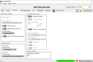
I am using ADC12DJ3200 operated in JMODE 0 with Fs=1250 MSPS. The Serdes is operated at 5 Gbps. FPGA Clock generated from LMK04828 is 125 Mhz (with DCLK=10). i am using ADC internal test mode patterns for my testing. Below is the screenshot of the JESD204B setting in the ADC GUI:
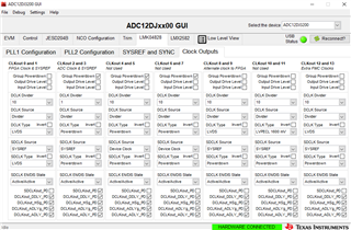
LMK04828 clock outputs are set as :
But when i program my adc device with this settings, my JESD link status is not getting up. Also sync signal is always low as shown below
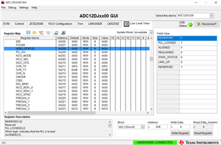
Am i missing anything here? Looking forward to your reply.

Regards

Rohit

  • Hi Rohit,

    In K28.5 test mode the ADC will transmits a continuous stream of K28.5 characters over and over and sync signal will remain low. The ADC is behaving as expected. Can you please clarify what are to trying to test? 

    Regards,

    Neeraj 

  • Hi Neeraj

    Thanks for your quick response.

    I am trying to perform interoperability of ADC12DJ3200 with my FPGA device using JESD204B. Currently i am testing with the internal test patterns and expecting them to be properly received at the FPGA side. But when i program the ADC card, the JESD link is not coming up as i showed through the screenshot in my previous post. Thanks on correcting me on the behavior of SYNC signal in case of K28.5 test mode but even if i try other test modes like ramp, repeated ILA etc, the SYNC signal is still low and JESD link is not up.

    I am curious to understand that why my JESD link is not coming up. I believe there is no issue with the clock as PLLs are properly getting locked, what am i missing here?

    Regards

    Rohit

  • Hi Neeraj

    Any inputs for me? Just to add, i am using JMODE0 and parameters are set based on Table 19 of ADC datasheet in the JESD Rx IP. Currently testing with 8 lanes configuration.

    Regards

    Rohit

  • Hi Rohit,

    You should be able check the status of PLLs on the FPGA side to make sure they are locked. 

    Can you also you have good electric connection for SYNC signal from the FPGA to ADC. To check  toggle the sync signal high and low on the FPGA side and make sure the BIT5 of register Address 0x208 is toggle as expected. 

    Regards,

    Neeraj 

  • Hi Neeraj

    PLL seems to be locked at the FPGA side, do you think clock needs to be measured here?

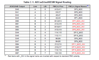
    About SYNC signal, i am doubtful on the mapping of this SYNC signal  from FPGA to ADC. In the ADC user guide i can only see mapping related to JESD output and FMC pins. I can't find how mapping related to SYNC signal needs to be taken care.

    Can you please suggest on this?

    Regards

    Rohit

  • Hi Rohit, 

    The SYNC_SE signal is connected to H31 pin on the FMC+ connector on the ADC EVM. You can download the ADC EVM schematic from ti.com using following link. 

    https://www.ti.com/lit/zip/slvc697

    Regards,

    Neeraj 

  • Hi Neeraj

    Thanks for the pointer to the ADC schematic, i took care about the SYNC signal mapping. But still JESD link status is not going up and SYNC signal is still low.

    >>Can you also you have good electric connection for SYNC signal from the FPGA to ADC. To check  toggle the sync signal high and low on the FPGA side and make sure the BIT5 of register Address 0x208 is toggle as expected. 

    I tried toggling the SYNC signal on the FPGA side from high to low (by default its always high) but still BIT5 of register address 0x208 stays low.

    Regards

    Rohit

  • Hi Rohit,

    This tells us that there not a good electrical connection between on sync signal between FPGA and ADC. You will first have have make sure you can fix the sync connection issue before you can move forward. 

    Regards,

    Neeraj