This thread has been locked.

If you have a related question, please click the "Ask a related question" button in the top right corner. The newly created question will be automatically linked to this question.

ADS4225EVM: Not all signal bits arrive to fpga

Part Number: ADS4225EVM
Other Parts Discussed in Thread: ADS4225

Hi

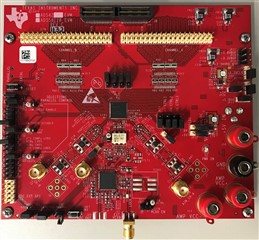
I have some issues getting signal from ADS4225EVM. This is the setup:
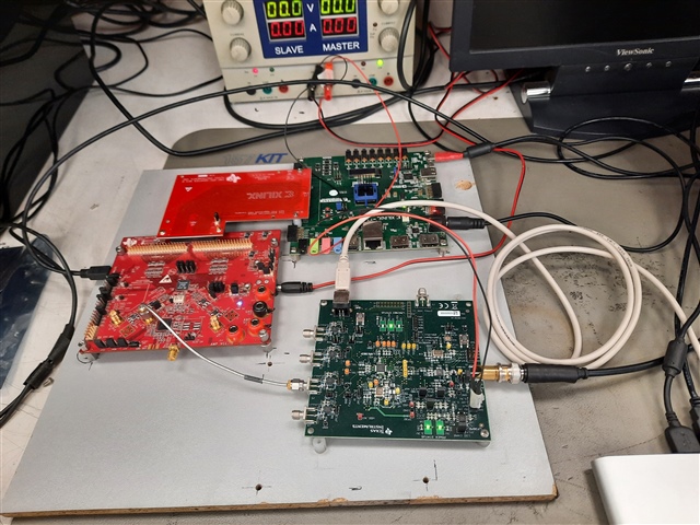
The stup consists:

  • SD1983EVK
  • ADC-FMC adapter
  • ADS4225EVM
  • Nexys Video (Based on Xc7-A200T)

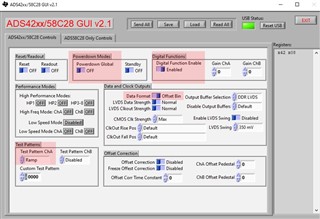
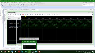
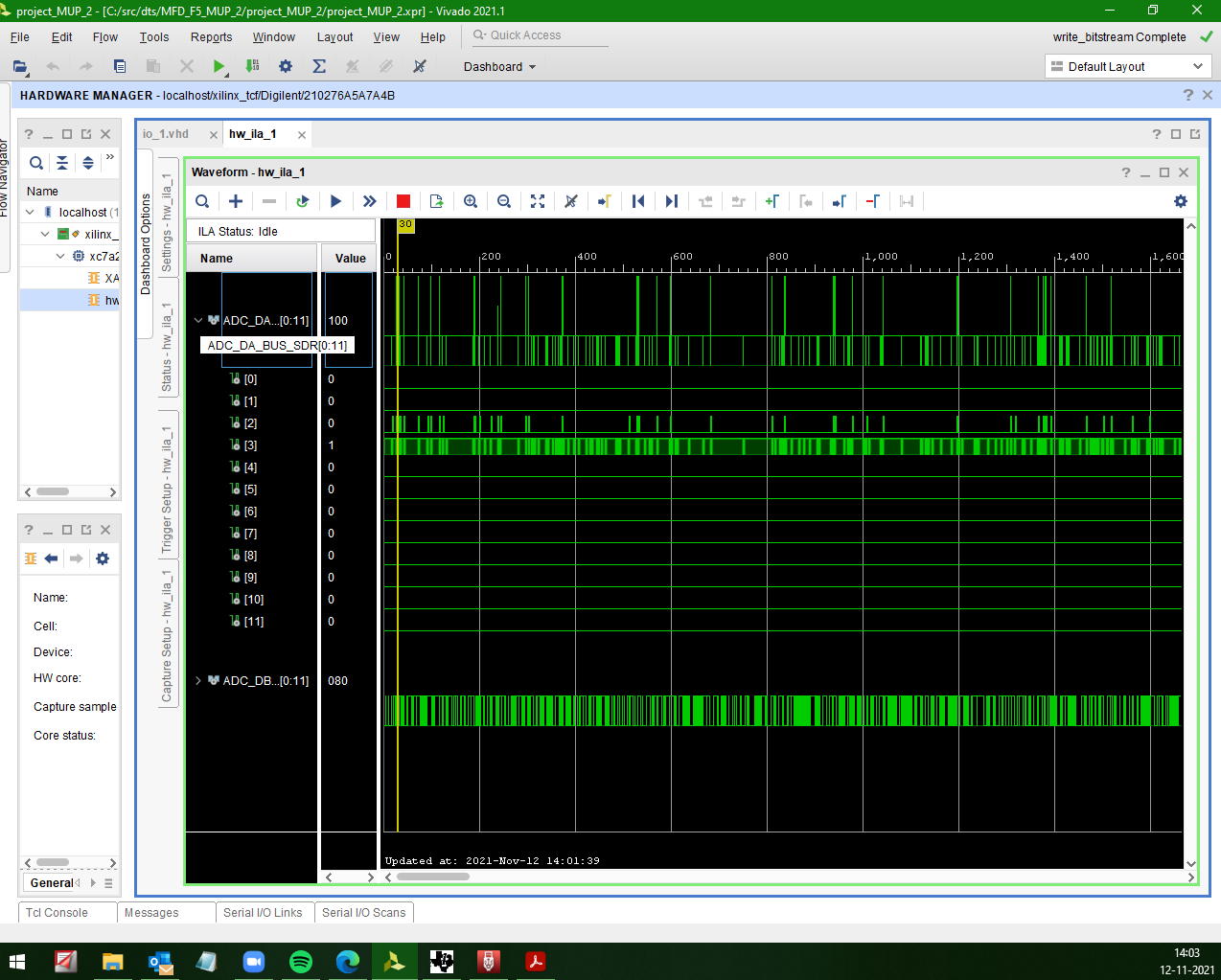
I'm getting just the third and fourth bits, but no others. I don't know why is this happening . Board has default settings and using the software I put on the ramp pattern generator. Instead of a ramp, I'm getting this:

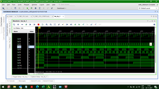
I made a simulation and I expected to see something like this:

I also ensured that the FMC voltage selector in the fpga side is set properly (1.8v), and mapping is apparently ok. Here's a table:

ADC-FMC     Nexys Video    
ADC ADS42XX J2 J1 FPGA
IO_0P N/C G9 FMC_LA_03_P
IO_0N N/C G10 FMC_LA_03_N
IO_1P DB12 G12 FMC_LA_08_P
IO_1N DB12 G13 FMC_LA_08_N
IO_2P DB10 H13 FMC_LA_07_P
IO_2N DB10 H14 FMC_LA_07_N
IO_3P DB8 G15 FMC_LA_12_P
IO_3N DB8 G16 FMC_LA_12_N
IO_4P DB6 H16 FMC_LA_11_P
IO_4N DB6 H17 FMC_LA_11_N
IO_5P DB4 G18 FMC_LA_16_P
IO_5N DB4 G19 FMC_LA_16_N
IO_6P DB2 H19 FMC_LA_15_P
IO_6N DB1 H20 FMC_LA_15_N
IO_7P DB0 H22 FMC_LA_19_P
IO_7N DB0 H23 FMC_LA_19_N
IO_8P DA12 G21 FMC_LA_20_P
IO_8N DA12 G22 FMC_LA_20_N
IO_9P DA10 G24 FMC_LA_22_P
IO_9N DA10 G25 FMC_LA_22_N
IO_10P DA8 H25 FMC_LA_21_P
IO_10N DA8 H26 FMC_LA_21_N
IO_11P DA6 H28 FMC_LA_24_P
IO_11N DA6 H29 FMC_LA_24_N
IO_12P DA4 G27 FMC_LA_25_P
IO_12N DA4 G28 FMC_LA_25_N
IO_13P DA2 C18 FMC_LA_14_P
IO_13N DA2 C19 FMC_LA_14_N
IO_14P DA0 H31 FMC_LA_27_P
IO_14N DA0 H32 FMC_LA_27_N
IO_15P D26 FMC_LA_28_P
IO_15N D27 FMC_LA_28_N
IO_16P G33 FMC_LA_31_P
IO_16N G34 FMC_LA_31_N
IO_17P G36 FMC_LA_33_P
IO_17N G37 FMC_LA_33_N
IO_18P H7 FMC_LA_02_P
IO_18N H8 FMC_LA_02_P
IO_19P H10 FMC_LA_04_P
IO_19N H11 FMC_LA_04_N
IO_20P C10 FMC_LA_06_P
IO_20N C11 FMC_LA_06_N
IO_21P D11 FMC_LA_05_P
IO_21N D12 FMC_LA_05_N
IO_22P C14 FMC_LA_10_P
IO_22N C15 FMC_LA_10_N
IO_23P D23 FMC_LA_23_P
IO_23N D24 FMC_LA_23_N
IO_24P C26 FMC_LA_27_P
IO_24N C27 FMC_LA_27_N
IO_25P G30 FMC_LA_29_P
IO_25N G31 FMC_LA_29_N
IO_26P H34 FMC_LA_30_P
IO_26N H35 FMC_LA_30_N
IO_27P H37 FMC_LA_32_P
IO_27N H38 FMC_LA_32_N
FCLKP G6 FMC_LA_00_P K18
FCLKN G7 FMC_LA_00_N K19
DCLKP D20 FMC_LA_17_P
DCLKN D21 FMC_LA_17_N
SDATA D17 FMC_LA_13_P
SCLK D18 FMC_LA_13_N
SPI_1 D14 FMC_LA_09_P
SEN D15 FMC_LA_09_N

Here's the rtl diagram that i'm using to digitize this:

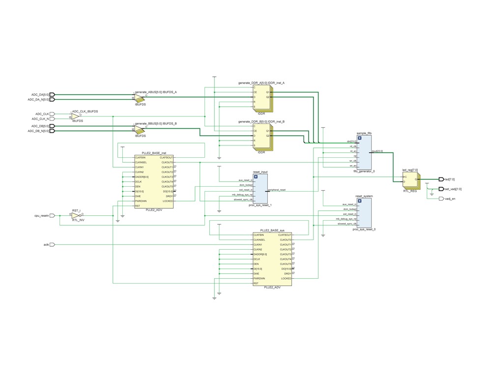
Any advice to get proper signal is welcome

Thanks

  • Hi Alejandro,

    I am checking into this and will get back to you soon. 

    Regards, Amy

  • Hi Alejandro,

    Could you check to see if the amplitude of the clock signal is at the level you expect? 

    You can also check that the clock data format is in agreement with the FPGA's clock expected format. Please refer to pg. 7 and Table 10 of the datasheet for the SEN Control Pin.

    https://www.ti.com/lit/ds/symlink/ads4225.pdf?ts=1637013539492&ref_url=https%253A%252F%252Fwww.ti.com%252Fproduct%252FADS4225 

    Regards, Amy

  • Clock configuration is ok. The CC pins expect .450v lvds swing. one of the adc options, so it's compatible and clock waveform at that pin appears to be correct. Also, I placed an ILA and a PLL in the fpga using the clock, and both fpga devices report no problems with clock.
    What other issue can be? can a faulty power rail (3.3, 1.8, 1.2) make signal unable to arrive properly formed to fpga? this power rail can be the power source of one of the fpga I/O banks?
    I can also show my code, it's still far from final application, so no copyright is involved yet

    Thanks

  • Hi Alejandro,

    Can you confirm that SPI writes are going through to the ADC by 1) issuing a power down SPI write and 2) confirming that the current on the EVM power supply goes down? It would also be good to probe the LVDS data outputs to see if there is activity.

    Faulty power rails could be an issue, if 1.8V ADC LVDS data lines are going to a 3.3V bank.

    Regards, Amy

  • Thanks for the advice Amy. Current does not go down when the software send the "Powerdown" command. It starts with .450A, but it remains still after "Powerdown" or "Suspend". Is there another measurement or test I can do?

    Regards,
    Alejandro Estay

  • Hi Alejandro,

    If the current remains unchanged with the global powerdown command, this indicates read/write issues with the SPI commands. I setup the ADS4225 with a TSW1400 capture card in our lab and captured a ramp test pattern.

    Here are things to check:

    1. Board jumpers
      1. Check that the jumpers are configured as described in the EVM user guide page 5, section 2.2: https://www.ti.com/lit/ug/slau333a/slau333a.pdf?ts=1637600064322&ref_url=https%253A%252F%252Fwww.ti.com%252Ftool%252FADS4225EVM
      2. I attached a picture of my jumper configuration for you to double check.

    Once you have confirmed that the jumpers are correctly set, try the global powerdown command again. On my board, the current decreases about 140 mA (from 680 mA to 540 mA) when this option is toggled.

    The other register writes that are needed to get the ramp test pattern capture:

    1. Digital Function Enable
      1. Toggle to 'Enabled'
      2. See datasheet pg. 56, section 9.3.3: https://www.ti.com/lit/ds/symlink/ads4225.pdf?ts=1637601761762&ref_url=https%253A%252F%252Fwww.ti.com%252Fproduct%252FADS4225
    2. Data Format
      1. Toggle to Offset Binary
    3. Test Patterns
      1. Select Ramp

    Let us know if you have other questions once you try these things out.

    Regards, Amy

  • Jumpers are apparently correct, but still spi commands are not working. SPI pins show activity, but there's only some subtle blinks. I check the "Readout" switch to get periodic updates and there's no periodic read activity in the pins.

  • Hi Alejandro,

    Can you verify that the SPI voltage signal levels and the setup and hold times are consistent with the ADS4225 datasheet?

    https://www.ti.com/lit/ds/symlink/ads4225.pdf?ts=1637694417880&ref_url=https%253A%252F%252Fwww.ti.com%252Fproduct%252FADS4225

    Regards, Amy

  • Hi Alejandro,

    Here is another thought:

    Try configuring the ADS4225EVM with the TI GUI first, instead of trying to control it with the FPGA. You can download it from the TI site here:

    • ADS42xxx SPI GUI (Rev. B)– SBAC113B.ZIP

    https://www.ti.com/tool/ADS4225EVM#tech-docs

    Once this is up and running, switch back to the FPGA SPI interface. If you have already tried this, trying comparing the voltage levels of the SPI signals when using the TI GUI vs. using the FPGA.

    Another option would be to use parallel programming mode for the ADC, which would allow the board to be configured without SPI. However, you would need to ensure that the FPGA interface is working before attempting any external SPI testing.

    Regards, Amy

  • To this moment i'm only controlling the ADC board with the GUI, and not from fpga. Can this serial interface malfunction be related to a problem with USB interface (FTDI)?

  • Hi Alejandro,

    To ensure that it is not a board issue, you can try running the board in parallel mode. Also, be sure to run the GUI as a 'system administrator'.

    Have you tried looking at the Device Manager to see if the USB is making a connection? You should see ‘USB Serial Converter’ listed under ‘Universal Serial Bus controllers’. If you unplug the USB, the device manager should blink. If this is not the case, it would be good to try a different USB port and/or cable.

    Regards, Amy

  • Thank you for your avice amy. Apparently was a misplaced jumper. Now i'm getting all bits into th fpga. They are not aligned so far, but I think is workable

    (the B channel is being tested with 1's pattern and all bits arrive. The upper is being tested with ramp. Is not a ramp, clearly, but is getting closer).

    In the ramp pattern all bits are used?

    Thanks

    ----------------------------------------------------------------------------------------------------------------------------------------------------------------------------------------------------------------------

    I switched boards (i have another nexys video) and some bits are "frozen". I switched back and another group of bits are frozen too. Can this be a problem with the FMC connection adapter? or is just problems with clock phase and adjustment in the fpga code?

  • Hi Alejandro,

    Yes I believe that all the bits are used for the ramp test pattern. One thing you can try is probing the outputs with a scope to test if there is possibly a bad connection with the FMC adapter.

    Regards, Amy

  • the A channel has all bits active. Also I moved the clock phase and I got correct signal (I think). Despite that B channel still has frozen bits. for my application is enough, so I will mark it as solved. Thanks Amy