This thread has been locked.

If you have a related question, please click the "Ask a related question" button in the top right corner. The newly created question will be automatically linked to this question.

ADS1292R: ADS1292R Works un-normal for EMG acquisition

Part Number: ADS1292R

Hi  

 I'm using ADS1292R to obtain EMG signal, I use only one channel--ch2 and I set Ch1 to power down mode.  during my dubug process, I found something that I can't understand,the following is my issues:

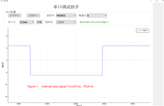
1: I'm sure my control code  for SPI bus works well, if I set chip internal test signal 1mV@1Hz, I can see the correct rusult.

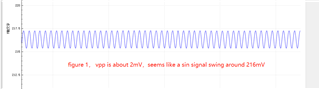
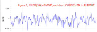
2: If I set MUX1[3:0] of  CH2SEL regesiter to 000( Normal electrode input) ,the adc results is shown as following figure 1(Y axis uint: mV,X axis unit : Sec):

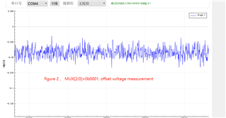
3:If I make input pins CH2P and CH2N shorted, the adc result is shown as following figure 2(Y axis uint :  mV,X axis unit : Sec):

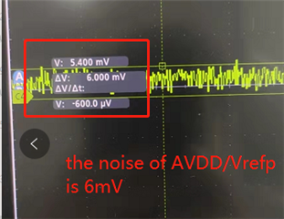
4: Vcap1 =1.2V, Vcap2 =4.99V,  AVDD = 3.0V,  DVDD=3.3V, and the voltage of RLDOUT is 2.92V(this voltage doesn't looks normal )

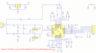
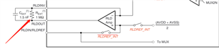
5: My sch file is shown as figure 3,

6:  If I shorted CH2P and CH2N ,or make CH2 in normal mode,  the output result of system should be a straight base line with a little fluctuation under the idle state。

Under this situation, I can never get EMG signal, the noise signal is too large for EMG signal,

Any help will be highly appreciated as I have limited time. Thank you

  • Hi Alex,

    Welcome to the E2E forum !!!

    The sine wave in Figure 1 is most likely due to the power line noise injection (50Hz/60Hz) in your system. You can verify this by looking at the power spectrum of the signals. The results from Figure 2 do not look correct when the input channel is shorted. By shorting the input INxP and INxN internally (MUX1[3:0] = 0b0001) or externally, you will be able to measure the offset voltage as well as the system noise performance. You can refer to Table 1 to 5 in the datasheet for the device noise performance in various data rates and gain setting.

    The RLDOUT voltage should be about mid-supply (VCM = 1.5V for your design) if no RLD_SENS (RLDxP/RLDxN) selection is connected. Please verify that you are setting the RLD amplifier correctly. Please also verify that the VREF is set correctly at 2.4V. The attached schematic looks fine; I do not see any significant issue with the design.

    Thanks

    -TC

  • Hi TCT,

    Thanks  a  lot  for your kindly help.

    The system is powered by a lithium battery, except there is a Vbus on the circuit of usb2usart (using usb2usart to send adc datas to pc)

    1,Yes, My system Vref = 2.425V,    I think this value of Vrefp is right. 

    2,the following figure 1 is interanl test signal ,U can see it's right, at this time, CONFIG2 = 0xA3; Ch2Sel = 0x05.

    3,Figure 2 is  MUX2[3:0] = 0b0001, U can see it's also probably right,  Vpp is about 25 uV, at this time, CONFIG2 = 0xA3; Ch2Sel = 0x01.

    But if  MUX2[3:0] = 0b0000 and I short CH2P and CH2N exteranlly, it works not normal. Now I think it's something wrong with my PCBA, maybe caused by the connection of AGND and GND, I'm not sure. If there is a problem here, Can you provide some layout guide more detailed than the spec?

    4,When comes to RLDOUT , it's controlled by regesiter  RLD_SENS and I usually set its valut to 0B0010_1100, under this condition, The RLDOUT always be 2.92V(pproximate value), if I set RLD_SENS= 0B0010_0000, VRLDOUT is 1.485V, but can system work well if RLD_SENS= 0B0010_0000? I do think it should be set RLD_SENS to 0B0010_1100 according to the spec. Maybe my point of this view is  wrong .

    Thanks for you help again and hope  to get your further advice.


  • Hi Alex,

    Thanks for the information. The internal test signals and the internal input-short results look fine. You should get a similar result to Figure 2 if you set the device to "normal electrode" mode and short both the INxP and INxN to the RLDOUT (VCM=1.5V).

    The RLDOUT is correct when you set the RLD_SENS to 0b0010_0000 where it is biased to the internal (AVDD+AVSS)/2. The use of RLDxP and RLDxN is to create a negative feedback loop by sensing the common-mode signal of a selected set of electrode and driving the body with an inverted common-mode signal. Please refer to section 8.3.10.2.4 for more details on the RLD drive circuit.

    It will be useful also to run the laptop using the battery to prevent any power line noise coupling from the USB connection. 

    Thanks

    -TC

  • Hi TCT,

    Thanks again for you advice.

    After listening to your suggestion, I have made  an attemptment  to short CH2P and CH2N to RLDOUT(I set register MUX2[3:0]=0b0000,  and RLD_SENS=0x2C) , and I found that the adc results were similar with the situation of MUX2[3:0]=0b0001 ,the output baseline is 0 mV and the vpp is about 40uV, which is shown the following figure 1,I think this result is right.

    The very strange thing is,when I shorted CH2P and CH2N to RLDOUT, the voltage of RLDOUT is 1.493V(AVDD/2), however, if I connect  CH2 channel electrodes and RLD electrode to my arm separately (I want to acquire EMG signal), The adc results of CH2 looks like the figure 1 of my original question. and the vlotage of RLDOUT is changed to about 0.18V, I don't know why this happened, maybe my power supply is unsufficient? I think if I set RLD_SENS=0x2C and RESP2=0x03, the RLDOUT will stay at the levle of AVDD/2(at least  slightly swing about AVDD/2, instead of 0.18V), Can  you provide some advice for this issue?

    Thank you very much and forward for you reply.

  • Hi Alex,

    Please check the power spectrum of the original Figure 1 and see what the dominant frequency of the signal is. What kind of electrode do you use to connect to your arm? Is it a wet or dry electrode? The RLD_SENS will sense the common-mode of a selected electrode set, and if there is any mismatch or significant offset at the inputs, the RLD feedback loop will fail and cause the common-mode voltage to be driven to either of the rails. Please note that you will need to optimize the RLD feedback loop to ensure the proper operation, depending on the design.

    Please see the link below for the app notes explaining how to improve the CMRR using the RLD drive.

    Improving Common-Mode Rejection Using the Right-Leg Drive Amplifier

    Thanks

    -TC

  • Hi,dear  TCT,

    Thanks again for your reply.

    I am sorry that we do not have dsp engineer in  our team. so I can't analyze the power spectrum of the original Figure 1 . 

    I think it's where the problem is,because I have measured the noise of AVDD/Vrefp/Vcap1, all Vpp of the noises are about 6mv, I think this noise level is  tolerable。But I can't confirm that whether the impedance of  electrode and my pcba is matched.

    if there is any mismatch or significant offset at the inputs

    1. Now my question is, how I check whether the electrode I used is qualified? Could you please provide a method to verify this issue? I read the manual of the EKG snap Lead ,it mentioned that the impedance between the electrode connector and the pcba plug is not more than 1 Ω, Is this a necessary condition for the system to work properly?  In the actual measurement, I found that this impedance is about 20 Ω.

    2.Refer to the documentation SBAA188 you provided, I think if there is any problem with the RLD feedback loop , I should adjust the value of Rexit (shown as following picture) of the feedback loop from 1MΩ to a a smaller value to reduce the closed-loop gain of the feedback loop,just like 500KΩ or a smaller Resistance, do you think this is a correct direction?

    Thanks very much for your help.

    Best wishes.

  • Hi Alex,

    I think you are going on the right path for the RLD design. I am not an expert on electrode design, so advice on this will be limited. Please consult with expert in the electrode design for further advice.

    Thanks

    -TC