This thread has been locked.

If you have a related question, please click the "Ask a related question" button in the top right corner. The newly created question will be automatically linked to this question.

ADS1261: CLKIN pin input capacitance

Part Number: ADS1261

Hi,

I am designing a digitizer board which will have 8 ADS1261. I am going to use one ASV-7.3728MHZ-EJ-T crystal clock oscillator as external clock to all of 8 ADS1261, but I didn't find the CLKIN pin input capacitance in the datasheet to certify that the ASV-7.3728MHZ-EJ-T will be able to drive the 8 CLKIN pins.

I would like a confirmation that this crystal clock oscillator PN will be OK for this application.

Thanks in advance,

Jorge

  • Hi Jorge,

    You can obtain the capacitance for any pin by using the IBIS model: https://www.ti.com/lit/zip/sbam375

    Out of curiosity, why not use the ADC's internal oscillator instead of an external clock? You should be able to use the ADC START pin or command to ensure that conversions all begin at the same time if that is the concern.

    -Bryan

  • Hi Bryan,

    Thank you for your quick reply.

    I found in the .ibs file a capacitance of 2.088pF (typical) for this pin, which would be too much considering 8 ADS1261 for that oscillator.

    We prefer to use an external clock for accuracy reasons, the ADS1261's internal oscillator can vary up to +/-2%. The ASV-7.3728MHZ-EJ-T has an overall frequency stability of +/-20ppm. And the ADC output data rate is important for this application.

    In this case, we though about using 2 ASV-7.3728MHZ-EJ-T, each one for 4 ADS1261. What do you think?

    Thank you, Bryan,

    Jorge

  • Hi Jorge,

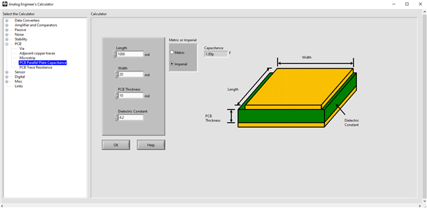
    One of the main considerations for the capacitive load on the clock is the board/trace capacitance. With so many devices it can be assumed that there would be a lot of trace capacitance seen by a single clock. You can google how to estimate trace capacitance or you can download our Analog Engineers Calculator and use the included tool (see the screenshot below): https://www.ti.com/tool/ANALOG-ENGINEER-CALC. This would be additive with the pin capacitance, and therefore 15pF may be insufficient even for 4x ADCs.

    There also looks to be an orderable option for the clock you selected that allows for a 50 pF output load drive capability. This could be an option if you have any doubts about the total capacitance seen by the clock. You might also reach out to the manufacturer to see what impact, if any, additional load capacitance has on the clock performance.

    Another option would be to use a clock fanout buffer at the output of your selected clock to add more drive strength to the system. The LMK00804BPW could be a good option, we have used this component on the EVMs for other devices in the past. Or you can reach out to our clocking team through the E2E forum for other suggestions / options.

    Please note that the 40kSPS data rate requires a different clock frequency (10 MHz), so you would not be able to use this data rate with the 7.3728 MHz clock you have selected.

    -Bryan

  • Hi Bryan,

    Thanks a lot for both your suggestions and comments.

    I downloaded TI's Analog Engineers Calculator (which is a really nice tool) and calculated the trace capacitance. Considering a 150mm length (which I think it will be possible considering just 4 ADCs), and the other parameters as you can see in the image below, the trace capacitance will be 7.84pF, with a total of 16.192pF. We know this can vary for many reasons, but I don't consider this as a problem.

    Regarding choosing the 50pF output load drive capability part number, it is possible, but, it looks like it is not common to find it.

    About the LMK00804BPW, it would be an option, thanks for suggesting, but I think we really can try to consider 2X ASV-7.3728MHZ-EJ-T and test the waveform and everything else to validate the design.

    Regarding the 40kSPS data rate, actually, we will use the analog circuitry and ADC configurations we already use in other project, and the output data rate is 2400SPS.

    Thank you again for you help and support.

    Best regards,

    Jorge

  • Hi Jorge,

    I am glad this information is helpful.

    It might make sense to include a footprint for a clock buffer in the first design iteration, as that will make it easier to populate later should you run into issues. Then, if you find you don't need it, you can always remove this footprint in the final design.

    -Bryan

  • Hi Bryan,

    Yes, good idea, I will do it.

    Thanks,

    Jorge