This thread has been locked.

If you have a related question, please click the "Ask a related question" button in the top right corner. The newly created question will be automatically linked to this question.

ADS1232: Interfacing of microcontroller with ADS1232

Part Number: ADS1232
Other Parts Discussed in Thread: ADS1230,

Hi,

    Can anyone share the programming code, which includes ADS1232 interfacing with microcontroller . Please also share schematic of ADS1232 interfacing with microcontroller.

Regards,

Shariq

  • Hi Sharique,

    We currently do not have example code for the ADS1232. However, the device is read-only so you should be able to follow the timing diagrams in Section 8.4.6 in the ADS1232 datasheet to get the ADC up and running.

    Similarly, for the connection to the MCU, you just need a DOUT and an SCLK line (and an optional PWDN pin).

    -Bryan

  • Hi Bryan,

                  Thanks for your reply. Actually there is example code regarding to MSP430 Micrcocontroller's interfacing with ADS1232 (or other ADSxxxx) in the form of TIDA, but i'm unable to find that on google.

    Best Regards,

    Sharique

  • Hi Sharique,

    As Bryan has mentioned the ADS1232 is a pin controlled device which requires no software configuration.  The original evaluation module for the ADS1232 is called the ADS1232REF and at one time we did provide the complete source code for this board.  However TI has decided that the original code did not comply with the current approval process and open source requirements.  We have been working on new code that can be used as an example, but due to some delays this will not be available until early next year.

    Depending on which processor you use the hardware abstraction layer will be somewhat different from one micro to another.  The connections to the hardware is easiest if you connect DRDY/DOUT to both the MISO of the micro and to an interrupt capable GPIO.  The falling edge of DRDY/DOUT should trigger an interrupt and the SPI interface is triggered to read 3 bytes of data within the interrupt routine.

    Some confusion may arise as there is no MOSI pin on the ADS1232.  In the end you just initiate the SCLK by writing to the internal TX buffer of the micro which starts the output of the SCLK even though the pin doesn't connect to anything.  Once the data has been transmitted read the byte from the RX buffer.

    The pseudo code would be as follows:

    • Set up the SPI peripheral and falling edge interrupt
    • Set continuous loop
    • If interrupt is triggered
      • Disable the interrupt
      • Place 0xff (value not important) in the TX buffer to initiate clocks
      • When the SCLKs have completed read the data to the MSB of data
      • Place 0xff (value not important) in the TX buffer to initiate clocks
      • When the SCLKs have completed read the data to the Mid-Byte of data
      • Place 0xff (value not important) in the TX buffer to initiate clocks
      • When the SCLKs have completed read the data to the LSB of data
      • Sign-extend the 24bit data to signed 32.
      • Clear and re-enable the interrupt (a flag can be set to check for new data within processing loop)
    • Do other processing events
    • Loop back

    Best regards,

    Bob B

  • Hi Benjamin Sir,

                          Thanks for your reply. I also got this link "https://e2e.ti.com/support/data-converters-group/data-converters/f/data-converters-forum/707409/ads1230-my-function-for-read-ads1230-help-me-pls/2608785#2608785"

    Let me try, then i'll back to you with results.

    Best Regards,

    Shariq Hussain

  • Hi Sharique,

    The referenced post use a bit-bang GPIO for the SPI communications to the ADS1230 (20-bit).  It would be much easier to use a built-in micro SPI peripheral when using the 24-bit ADS1232.

    Best regards,

    Bob B

  • Hi Benjamin Sir,

         It means using SPI peripheral of microcontroller is easier than using the bit-bang GPIO. Here i want to ask that microcontroller's MISO should be connected to ADC's DOUT/DRDY, microcontroller's SPI CLK should be connected to ADC's SCLK pin & which pin of microcontroller should be connected to ADC's PDWN.

    Best Regards,

    Shariq Hussain

  • Hi Shariq,

    Your SPI connections are correct.  The MOSI pin from the micro can be left floating.  The PDWN pin can be connected to any available GPIO pin on the micro.

    Best regards,

    Bob B

  • Hi Benjamin Sir,

                           Actually parallely we are engage with Esp Ble Mesh, Sorry for the delay. we are going to use three pins of microcontroller for interfacing with ADS1232.

    MISO,SCK,Ext Int are the three pins. We configure SPI in master mode. Firstly to initiate serial clock we have to send a dummy byte via Tx Buffer. But in master mode we just receive the data via MISO pin. So, how to send dummy byte via MISO pin.

    Best Regards,

    Shariq Hussain 

  • Hi Shariq,

    Even though you are not using the MOSI pin on the micro, you can still initiate the SCLK for writing a dummy byte(s) to the TX buffer of the micro you are using.

    Best regards,

    Bob B

  • Hi Bob Sir,

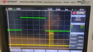
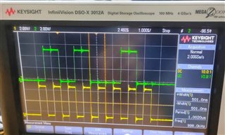
                      Why every time i received 0xFF? Also see the attached signals. In firmware i follow your steps. Initialize SPI as Master with frequency 1 MHz. 

    while (1) // Ideal loop tasks
    {
              IWDG_KR = 0xAA; //Reset IWDG down counter to FF

              if (FallingEdgeDetect == 1)
             {
                   PD_CR2 &= 0xFB; // Disable PD2 As External interrupt

                    while ((SPI_SR & SPI_FLAG_TXE) == 0x00){} // Wait until end of transmit
                    SPI_DR = 0x52; // Send a Dummy byte
                    while ((SPI_SR & SPI_FLAG_RXNE) == 0x00){} // Wait the byte is entirely received by SPI
                    data1 = SPI_DR; // Store the received byte in the RxBuffer

                    while ((SPI_SR & SPI_FLAG_TXE) == 0x00){} // Wait until end of transmit
                    SPI_DR = 0x52; // Sent a Dummy byte
                    while ((SPI_SR & SPI_FLAG_RXNE) == 0x00){} // Wait the byte is entirely received by SPI
                    data2 = SPI_DR; // Store the received byte in the RxBuffer

                    while ((SPI_SR & SPI_FLAG_TXE) == 0x00){} // Wait until end of transmit
                    SPI_DR = 0x52; // Sent a Dummy byte
                    while ((SPI_SR & SPI_FLAG_RXNE) == 0x00){} // Wait the byte is entirely received by SPI
                    data3 = SPI_DR; // Store the received byte in the RxBuffer

                   PD_CR2 |= 0x04; // Enable PD2 As External interrupt

        FallingEdgeDetect = 0;
    }

    @far @interrupt void EXTI_PORTD_IRQHandler (void)
    {
             FallingEdgeDetect = 1;

             return;
    }

    Best Regards,

    Shariq Hussain

  • Hi Shariq,

    If I understand the scope shots correctly the left picture is showing MISO and the right picture is showing MOSI from the micro.  The first issue I see is only 8 clocks are transmitted and not the entire 24 for the data.  The second issue is the micro is using the wrong phase.  The ADS1232 transitions on the rising edge of SCLK and remains steady on the falling edge.  This is sometimes referred to as Mode 1 SPI.  You are using Mode 0 which transitions on the falling edge and stays steady on the rising edge.  You will need to change the phase of your SPI to the correct mode.

    I do not see any data that is showing 0xFF, in fact it would appear that the first byte of data is 0x00.  It would be helpful to see all of the data and not just one byte.  It would also be helpful to see your schematic.  You must make sure that you have AVDD and DVDD at nominal operating voltage and an appropriate reference connected.  All digital inputs should be connected to some specific logic level and not left floating.  The PDWN pin must also be set to high.

    Without attempting to read data, you can verify that the ADS1232 is operating by monitoring DRDY/DOUT and you should see the conversion ready signal toggle at the selected data output rate selected by the SPEED pin setting.

    Your code is showing the use of the same register for both transmit and receive.  This may be correct for your micro, but I would suggest that you verify that the register you are using is the correct one for the micro.  Also, you are clearing the transmit buffer before you place the dummy byte into the register.  Normally I would expect the byte to be placed into the register before checking to see if the buffer is empty.  I would verify that that is the correct procedure.

    Also in your interrupt routine you do not clear the interrupt.  Usually this is required to prevent the interrupt from re-entering the interrupt continuously.  I would suggest verifying that the interrupt is cleared after each time it is entered.

    I hope this gives you some idea on what to check and how to verify the data.

    Best regards,

    Bob B

  • Hi Bob Sir,

         Plese find attached Schematic & zip files containing images and video.

    => Here i attached the schematic of a running circuit in which PIC microcontroller interfaces with ADS1232. Microcontroller's 3 pin used for interfacing &       all the three pins are normal GPIO, means no SPI functionality on those pins.Practically using oscilloscope i observed that PDWN continous remains       high & signal of SCLK & Dout/Drdy is in the attached image. SCLK frequency is 117.7 KHz, +width is 5.7 uSec and -width is 2.7 uSec. Complete             duration of 24 clk pulses is 200 uSec. And this cycle repeats after every 100 msec. And there is also small width 25th pulse as comparison to 24 clk         pulses.Please see all pics with patience for better clearance.Green signal is SCLK, Yellow is DOUT & blue is PDWN.
         This is a market purchased circuit.

    => Now what i did, cut the tracks of DOUT & SCLK on PCB to break the communication between PIC mcu & ADS1232. And connect my development           kit with ADS1232 by using 3 wires. Two wires from the same ADS's pin DOUT, one goes to mcu's ext interrupt GPIO & other goes to mcu's MISO.           And third wire SCLK to mcu's SCLK. In firmware i initialize SPI as master with frequency 1 MHz.Frame Format : MSB is transmitted first, Clock                 polarity is 0: SCK to 0 when idle.Development kit's VDD (+5V) & VSS connected to that circuit. Not used PDWN from my mcu as it reamins high by         PIC mcu. Please see all pics & one video with patience for better clearance.Green signal is SCLK, Yellow is MISO & blue is MOSI.

    => I send 0x52(dummy byte) by MOSI. As transmission is 8 bits, may be this the reason of 8 clk pulses.

    => Yes you are correct, phase of SPI is wrong.So, i correct that.In firmware SPI initialization,Now Clock phase is 1: The second clock transition is the            first   data capture edge

    => SPI_DR – Data Register
         The data register is used in two contexts, when data has been received and to transmit data. Reading this register will retrieve data from the receive         buffer. Setting this register will load the specified value into the transmit buffer.

    => As per your suggestion now i first send dummy byte then wait for clearing the Tx Buffer. After Receiving data wait for clearing the Rx Buffer.

    => There is no documented register for clearing external interrupt. Ext Int works fine for our remote protocol, means no issue.


    while (1) // Ideal loop tasks
    {

       if (FallingEdgeDetect == 1)
       { 
              PD_CR2 &= 0xFB; // Disable PD2 As External interrupt

              SPI_DR = 0x52; // Sent a Dummy byte
              while ((SPI_SR & SPI_FLAG_TXE) == 0x00){} // Wait until end of transmit
              data1 = SPI_DR; // Store the received byte in the RxBuffer
              while ((SPI_SR & SPI_FLAG_RXNE) == 0x00){} // Wait the byte is entirely received by SPI


              SPI_DR = 0x52; // Sent a Dummy byte
              while ((SPI_SR & SPI_FLAG_TXE) == 0x00){} // Wait until end of transmit
              data2 = SPI_DR; // Store the received byte in the RxBuffer
              while ((SPI_SR & SPI_FLAG_RXNE) == 0x00){} // Wait the byte is entirely received by SPI

              SPI_DR = 0x52; // Sent a Dummy byte
              while ((SPI_SR & SPI_FLAG_TXE) == 0x00){} // Wait until end of transmit
              data3 = SPI_DR; // Store the received byte in the RxBuffer
              while ((SPI_SR & SPI_FLAG_RXNE) == 0x00){} // Wait the byte is entirely received by SPI

              PD_CR2 |= 0x04; // Enable PD2 As External interrupt

              FallingEdgeDetect = 0;
       }

    }


    @far @interrupt void EXTI_PORTD_IRQHandler (void)
    {
        FallingEdgeDetect = 1;

       return;
    }

    PIC(mcu)-ADS1232.rarMy(mcu)-ADS1232.rar3364.Schematic.PDF

    Best Regards,

    Shariq Hussain

  • Hi Shariq,

    Thanks for the additional information.  The device is operating at 10sps which results in 100ms conversion results.  So at this point do you have any issues as it appears to be working as expected?

    The gain is set to a gain of 2, and the schematic is not clear at to what the input is or the voltage applied.  So I cannot tell what to expect with respect to the codes.

    Best regards,

    Bob B

  • Hi Bob Sir,

                   Voltage applied is +5V. Here is my few queries as per comparison between Market purchased running circuit (PIC mcu) & our mcu interfacing : 

    => In PIC mcu folder, it's clearly seen that 25 clk pulses used & i'm using 24 pulses. Why?

    => In PIC mcu folder, simple GPIO pins are used, 25 clk pulses without any gap. I'm using SPI clk pin so in packet of 24 clk pulses there is gap between each 8 clk pulse. Why? 

    => In PIC mcu folder, data and clk combination repeats after every 100 msec. But in my case there is unexpected behaviour means no perfect interval.    Why?

    => In PIC mcu folder, after every 100 msec DOUT pin goes from high to low and after 25th clock pulse DOUT pin goes to high state. But in our case there is different behaviour that can be seen in video that sent to you.

    Best Regards,

    Shariq Hussain

  • Hi Shariq,

    I would suggest reviewing the ADS1232 datasheet.  I will attempt to answer your questions.

    => In PIC mcu folder, it's clearly seen that 25 clk pulses used & i'm using 24 pulses. Why?

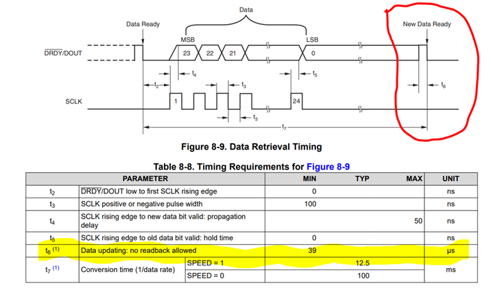
    Apparently the original implementation was using a polling method for the end of conversion instead of an interrupt method.  This means that the DRDY/DOUT output must be forced high to be able to recognize that the conversion has completed which appears as a high to low transition on DRDY/DOUT.  The reason is the LSB of the last conversion read could be either high or low.  If it is low, then a polling loop could easily misinterpret the low output as a new conversion.  Using an interrupt is the preferred method as the high to low transition always occurs on DRDY/DOUT regardless of the previous state of the pin.  Please see the ADS1232 datasheet on page 24 and figures 8-9 (showing the new data ready transition following the end of conversion ) and 8-10 (showing DRDY/DOUT going high after 25th clock).

    => In PIC mcu folder, simple GPIO pins are used, 25 clk pulses without any gap. I'm using SPI clk pin so in packet of 24 clk pulses there is gap between each 8 clk pulse. Why? 

    The original implementation shows a 'bit-bang' approach using the GPIO pins.  This requires a unique set of functions that actually takes a specific amount of processor time to complete and once started should not be interrupted.  The peripheral is usually running independently of the main processing loop.  This provides a near 50/50 duty cycle which is preferred.  The bit-bang approach is related to timing of the function and can be interrupted by other processing steps.  When using the SPI peripheral there can be delays between transmitted bytes depending on the usage.  In your case there is space created while waiting for the TX buffer to empty and the RX buffer to be ready to read (cause by the 'while' conditions).  It does not hurt to have these small spaces of time between bytes being read from the device.

    => In PIC mcu folder, data and clk combination repeats after every 100 msec. But in my case there is unexpected behaviour means no perfect interval.    Why?

    The ADS1232 is completing the conversion every 100ms, but you may not be reading it when it completes.  Make sure that your interrupt is triggering on the falling edge (high to low) transition of DRDY/DOUT.  Also make sure that your total processing loop time does not take more than 100ms to complete or you will miss data.  There can be loop delays if you are transmitting data to a COM terminal or some other display.  I noticed in the video that the scope was triggering on about 1 second intervals instead of 100ms.  Have your scope trigger on the falling edge of the channel for DOUT/DRDY.  I think that you will find that you are not capturing all of the data, but the conversion is completing on 100ms intervals.

    => In PIC mcu folder, after every 100 msec DOUT pin goes from high to low and after 25th clock pulse DOUT pin goes to high state. But in our case there is different behaviour that can be seen in video that sent to you.

    Yes, this is what I was expressing in my first answer.  24 SCLKs is the data.  A 25th clock will force DRDY/DOUT high.  If 26 or more clocks are sent the ADS1232 will enter a self-offset calibration cycle which at the 10sps data rate will take about 8 conversion cycles (800ms) to complete and provide the appropriate conversion result for the selected input.  As mentioned earlier, the conversion LSB can either be high or low, and when polling the pin by GPIO you need to force this pin high.  When using an interrupt driven system you monitor for a falling edge on DRDY/DOUT and has no dependence on the previous state of DRDY/DOUT.

    Best regards,

    Bob B

  • Hi Bob Sir,

                   As per my understanding, what is my mistake that  generation of the 25th clock pulse required. So, the DOUT pin goes high. And then wait for high to low transition of DOUT pin which will happens after 100 msec.

    Query 1 :=> So, for the 25th pulse what i have to do? Because if again i send a dummy byte after 24 clk pulses then it's the generation of 8 more clk pulses. Means total 30 clk pulses.

    Query 2 :=> I also saw your previous answers on forum in which you suggested that GPIO bit bang approach is easier than SPI peripheral. But you told me that SPI peripheral is better than GPIO bit-bang approach. you also suggested a link for firmware guidance, but on clicking link webpage not responding. For this please check the attached image 

    Best Regards,

    Shariq Hussain

  • Hi Shariq,

    There is still a disconnect in my explanation and I apologize that I am not clear or do not fully understand your use case.  If you do not collect any data from the ADS1232 you will see with the SPEED pin set low (as shown in the schematic you provided) that DRDY/DOUT will pulse low-high-low every 100ms.

    The DRDY/DOUT will always transition from either high - low or low - high - low after the completion of every conversion.  Depending on the last bit transmitted in the data the output may already be high so that only the high-low transition is seen.  If the last bit transmitted is low, then the action will be low-high-low.  This is shown in the datasheet on page 24.

    The update period is shown as a minimum time of 39us where the conversion result is placed into the output buffer to be transmitted on DRDY/DOUT.  I captured the following screen shot from your video as a demonstration.

    Notice that the interrupt worked on the high-low transition on DRDY/DOUT and your code recognized that the new data was available to be read from the ADS1232.  So I hope this is more clear as to why 25 SCLKs are not necessary to determine that new data is available. 

    Consider also that the ADS1232 device is about 15 years old and that many older micros were very slow and perhaps where not GPIO interrupt capable.  If this is the case then a polling loop for monitoring the state of the DRDY/DOUT is used.  In this case the micro processing loop may be too slow to recognize the 39us transition time for low-high-low transition which would then require a longer time period to determine that DRDY/DOUT actually made a low-hgh-low transition.  For this specific use case, the bit-bang approach was required and the use of the 25th SCLK forces the DRDY/DOUT high.  The best method to use would be the interrupt method (which is also used on the ADS1232REF) and not the bit-bang approach and 25 SCLKs.

    Query 1 :=> So, for the 25th pulse what i have to do? Because if again i send a dummy byte after 24 clk pulses then it's the generation of 8 more clk pulses. Means total 30 clk pulses.

    Don't use the 25 SCLK as your code is working already as shown in the picture above.  If you send an extra byte (actually 32 clocks and not 30) you will place the ADS1232 into self-offset calibration which takes 800ms to complete.

    Query 2 :=> I also saw your previous answers on forum in which you suggested that GPIO bit bang approach is easier than SPI peripheral. But you told me that SPI peripheral is better than GPIO bit-bang approach. you also suggested a link for firmware guidance, but on clicking link webpage not responding.

    As I stated previously, the ADS1232 is now about 15+ years old and the response you are referring to is also quite old.  The ftp server was shut down shortly after the response as shown in your post took place due to IT security reasons.  Software on the ftp server was 'grandfathered' to not require certain standards for software release as they pertain to certain legal requirements from TI.  So the link and software are no longer available in its previous form.  I am currently working on updating example code which will be placed eventually on the product page for the ADS1232, but that will be at least 6 weeks away. 

    As I also stated previously, the TI code you referred to was interrupt driven and not bit-bang.  So I would advise you to continue with the code you are using and optimize it.  The referred to post requested information on a particular competitor processor which I did not know how to setup the SPI peripheral or if an interrupt capable GPIO pin was available.  So in this particular customer use case it may have been easier to use the bit-bang approach.  I would never recommend using a bit-bang approach if an interrupt method is available.

    As the ADS1232 has no registers and is pin controlled, it is not a complicated device to use (although you may think it is) compared to other ADCs.  Follow the datasheet and the information regarding setup and timing and you have all of the information you need to collect the data.  The forthcoming example code will not be much different than what you have already posted in this thread.  The most difficult portion of the code is the hardware abstraction which is processor dependent as it relates to the SPI peripheral and communication.

    Best regards,

    Bob B

  • Hi Bob Sir,

                    Please check the attached zip folder i.e., "Result" :

    1 => Thanks for your guidance for firmware, as i got result. Please verify images of "Result" folder, to confirm that it's right.

    2 => At firmware side i did a little bit change i.e., waiting for clearance of Tx/Rx buffer before sending/receiving respectively. As per doing this i read exact bytes as per signal.

    3 =>  Folder also contains a schematic of ADS1232 alongwith nearby hardware integration. Currently i havn't pressure sensor, it will take upto 10 days to deliver to me. Till now connector is open & what we are reading is a garbage or float value. So for self testing, here can i give a 100 milliVolt signal to 1st pin of PL11 connector & GND to 2nd pin of PL11 connector?  

    4 => In normal mcu inbuilt ADCs like 10 bit or 12 bit, we simply have idea that on this particular analog volt we got this particular value of counts. So, if we give a 100 milli Volt signal on PL11 connector, what we got at the output of ADS1232.

    Best Regards,

    Shariq HussainResult.rar

  • Hi Shariq,

    It appears that the code is reading correctly now from the ADS1232.  As to your schematic, I'm not sure how this circuit is intended to work.  The input has a DC blocking capacitor C5A and the ADS1232 is designed to measure DC or near DC signals.

    As to the conversion of code to volts, this is shown in the datasheet on page 23.  One LSB (or one code) is equal to (0.5 VREF / Gain) / (223 – 1).  The schematic is showing that the GAIN0 pin is pulled high which is a gain of 2.  The reference voltage is shown as 5V.  So the value of 1 code is equal to ((0.5 * 5V / 2) / (8388607) = 149nV.  The input voltage is determined by the number of ADC codes (24 bit value) times the value of 1 code.  For a 100mV input you should see codes around 671141 decimal or 0x0A3DA4.  However, with the C5A cap installed it is difficult to say what value to expect.

    Best regards,

    Bob B