Dear Technical Support Team,
I have six questions for ADC3643.
Q1 In 8.5 on page 43 of the data sheet, it is stated that it can be operated in the default mode without being controlled by SPI. What is the default interface mode?
The device is primarily configured and controlled using the serial programming interface (SPI) however it can
operate in a default configuration without requiring the SPI interface
Q2 Is the default value of the register the value listed in the Reset column of each register value table?
Also, is the default state different from the default value in the register?
(For example, it is stated that 000 is returned until it is written by SPI at [2: 0] at address 0x07).
Q3 What is the state of the pins before DCLKIN selects 2wire mode in SPI (In, Out, Hi-Z)?
If it is Out when the power is turned on, do we need to be able to avoid output collisions?
Q4 Regarding the explanation of Bit0 of register 0x13 on page 51, is 0x12 in the part of "... Register 0x07 along with the E-FUSE Load (0x12, D0) ..." a typo of 0x13?
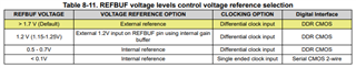
Q5 Regarding REFBUF, if the differential clock is set by External reference and the 2wire mode is set by SPI, is 8.5.1 on page 43 particularly irrelevant?
Also, when making the above settings in SPI, is there any recommendation for processing on the circuit of the REFBUF pin?
Q6 InitializeSetUp on page 64 requires 200,000 clocks for calibration. Do I need DCLKIN at this time?
Best Regards,
ttd