Hello,
We are using ADS1261 to sample magnetometers in our design by configuring the sensors as differential inputs. Our code can read/wright registers and fetch samples from the sensors. To validate if the chip works correctly, we have test code to setup as below and read the differential signal of either: (AVDD-AVSS)/4 - DVDD/4, or DVDD/4 - (AVDD-AVSS)/4. Unfortunately we cannot get expected values.
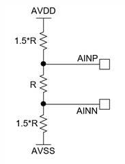
1. In our design: AVDD = 5.0VDC; AVSS = gnd; DVDD = 3.3VDC. Reference is set to internal 2.5VDC. All the three voltage pins work correctly with the right readings from a multimeter.
2. The ADC is set to:
[MODE0] = 0b01001000: 1200 SPS, sinc1
[MODE1] as default, 0b00000001: chop mode off, continuous conversions, 50us delay
[MODE3] as default, 0x00h
[REF] = 0b00010000: 2.5V Internal Reference
[OFCAL0] as default, 0x00h
[OFCAL1] as default, 0x00h
[OFCAL2] as default, 0x00h
[FSCAL0] as default, 0x00h
[FSCAL1] as default, 0x00h
[FSCAL2] as default, 0x40h
[IMUX] as default, 0xffh
[IMAG] as default, 0x00h
[PGA] = 0b00000000: gain 1
[INPMUX] = 0b11001101: Positive_Input_Multiplexer=(AVDD-AVSS)/4=5.0VDC/4; Negative_Input_Multiplexer=DVDD/4=3.3VDC/4.
[INPBIAS] as default, 0x00h
3. The test code is applied RREG commands to read back all the registers with 3 bytes to validate the setups. All readings are right as below:
RREG ID: FF=0xff; B1_20h=0x20; B2_8xh=0x81
RREG STATUS: FF=0xff; B1_21h=0x21; B2_05h=0x05
RREG MODE0: FF=0xff; B1_22h=0x22; B2_48h=0x48
RREG default MODE1: FF=0xff; B1_23h=0x23; B2_01h=0x01
RREG default MODE2: FF=0xff; B1_24h=0x24; B2_00h=0x00
RREG default MODE3: FF=0xff; B1_25h=0x25; B2_00h=0x00
RREG REF: FF=0xff; B1_26h=0x26; B2_10h=0x10
RREG default OFCAL0: FF=0xff; B1_27h=0x27; B2_00h=0x00
RREG default OFCAL1: FF=0xff; B1_28h=0x28; B2_00h=0x00
RREG default OFCAL2: FF=0xff; B1_29h=0x29; B2_00h=0x00
RREG default FSCAL0: FF=0xff; B1_2ah=0x2a; B2_00h=0x00
RREG default FSCAL1: FF=0xff; B1_2bh=0x2b; B2_00h=0x00
RREG default FSCAL2: FF=0xff; B1_2ch=0x2c; B2_40h=0x40
RREG default IMUX: FF=0xff; B1_2dh=0x2d; B2_ffh=0xff
RREG default IMAG: FF=0xff; B1_2eh=0x2e; B2_00h=0x00
RREG PGA: FF=0xff; B1_30h=0x30; B2_00h=0x00
INPMUX: FF=0xff; B1_31h=0x31; B2_cdh=0xcd
RREG default INPBIAS: FF=0xff; B1_32h=0x32; B2_00h=0x00
4. Then the START command is issued.
5. Then the RDATA command and RREG to get STATUS command are applied to read the differential signal + status at 1KHz. The debug printings are
RADTA: B0_FF=0xff; B1_12h=0x12; B2_MSB=0x7f; B3_MID=0xff; B4_LSB=0xff; result= 8388607
STATUS: FF=0xff; B1_21h=0x21; B2_05h=0x05
RADTA: B0_FF=0xff; B1_12h=0x12; B2_MSB=0x7f; B3_MID=0xff; B4_LSB=0xff; result= 8388607
STATUS: FF=0xff; B1_21h=0x21; B2_05h=0x05
RADTA: B0_FF=0xff; B1_12h=0x12; B2_MSB=0x7f; B3_MID=0xff; B4_LSB=0xff; result= 8388607
STATUS: FF=0xff; B1_21h=0x21; B2_05h=0x05
There are 2 questions for the result:
1) 0x7fffff = 8388607 is 2.5V, which is not the expected value: 5.0V/4 - 3.3V/4 = 0.425V.
2) It seems there is overflow since we always get 0x7fffff. But STATUS of 0x05 isn't indicated it.
6. For the above test, we change [INPMUX] = 0b11001101 to 0b11011100 for:
Positive_Input_Multiplexer=DVDD/4=3.3VDC/4; Negative_Input_Multiplexer=(AVDD-AVSS)/4=5.0VDC/4.
The debug printings are:
RADTA: B0_FF=0xff; B1_12h=0x12; B2_MSB=0xde; B3_MID=0xc6; B4_LSB=0xc8; result= -2177336
STATUS: FF=0xff; B1_21h=0x21; B2_05h=0x05
RADTA: B0_FF=0xff; B1_12h=0x12; B2_MSB=0xde; B3_MID=0xdb; B4_LSB=0x0b; result= -2172149
STATUS: FF=0xff; B1_21h=0x21; B2_05h=0x05
RADTA: B0_FF=0xff; B1_12h=0x12; B2_MSB=0xde; B3_MID=0xc9; B4_LSB=0x95; result= -2176619
STATUS: FF=0xff; B1_21h=0x21; B2_05h=0x05
RADTA: B0_FF=0xff; B1_12h=0x12; B2_MSB=0xde; B3_MID=0xd3; B4_LSB=0x16; result= -2174186
STATUS: FF=0xff; B1_21h=0x21; B2_05h=0x05
RADTA: B0_FF=0xff; B1_12h=0x12; B2_MSB=0xde; B3_MID=0xd5; B4_LSB=0xdf; result= -2173473
STATUS: FF=0xff; B1_21h=0x21; B2_05h=0x05
The result is around -2177336 (guess noise introducing changes).
The expect value is: (3.3V/4 - 5.0V/4) X 0x7fffff / 2.5V = -1426063.
The sample value seems partly reasonable even it's not close to the expected.
7. For the above test with Steps 1~6, we change [PGA] = 0b00000001 to have gain of 2 for another test.
1) for step 5 we get debug printings as
RADTA: B0_FF=0xff; B1_12h=0x12; B2_MSB=0x7f; B3_MID=0xff; B4_LSB=0xff; result= 8388607
STATUS: FF=0xff; B1_21h=0x21; B2_05h=0x25
Although result of 0x7fffff = 8388607 has no change, PGAL_ALM bit of STATUS is set to high to indicate overflow.
2) for step 6 we get debug printings as
RADTA: B0_FF=0xff; B1_12h=0x12; B2_MSB=0xbd; B3_MID=0x97; B4_LSB=0xc1; result= -4352063
STATUS: FF=0xff; B1_21h=0x21; B2_05h=0x05
RADTA: B0_FF=0xff; B1_12h=0x12; B2_MSB=0xbd; B3_MID=0xb5; B4_LSB=0xdc; result= -4344356
STATUS: FF=0xff; B1_21h=0x21; B2_05h=0x05
RADTA: B0_FF=0xff; B1_12h=0x12; B2_MSB=0xbd; B3_MID=0x92; B4_LSB=0x84; result= -4353404
STATUS: FF=0xff; B1_21h=0x21; B2_05h=0x05
RADTA: B0_FF=0xff; B1_12h=0x12; B2_MSB=0xbd; B3_MID=0xb1; B4_LSB=0x03; result= -4345597
STATUS: FF=0xff; B1_21h=0x21; B2_05h=0x05
Result of -4352063 is roughly doubled value as of results in step 6. This is expected since the gain is doubled.
Summarized questions to ask your help please:
1. Why cannot get the sample values when [INPMUX] = 0b11001101?
2. Why cannot get the accurate sample values when [INPMUX] = 0b11011100?
Regards,
Bin