This thread has been locked.

If you have a related question, please click the "Ask a related question" button in the top right corner. The newly created question will be automatically linked to this question.

ADS5287: Application notes or sample code for initialization sequence of configuration registers

Part Number: ADS5287
Other Parts Discussed in Thread: TLA2518, AFE5809

Hi Team,

Our customer is having a communication problem with ADS5287 and he is looking for an application notes regarding the initialization sequence of configuration registers. Do we have a sample code for ADS5287?

Regards,

Danilo

  • Hi Danilo,

    I am checking into this and will get back to you soon.

    Regards, Amy

  • Hi Amy,

    Thank you for your response. We will wait for your update.

    Regards,

    Danilo

  • Hi Danilo,

    The initialization sequence can be found on pg. 3 of the ADS5287 datasheet under “Initialization Registers”. If the issue is with SPI communication, you can try writing / reading to the power down register. 

    Regards, Amy

  • Hi Amy,

    I have shared this information to our customer but he can't communicate with the device. Do we have sample code showing the configurations of registers?

    Regards,

    Danilo

  • Hi Danilo,

    First, a reset should be done (this can be done with the HW using the reset button, or in software, by writing 0x0001 to address 0x00).

    Try having the customer write 0x00A0 to address 0x0F: (SPIWRITE 0x0F  0x00A0, and SPIREAD 0x0F should return 0x00A0).

    If this is unsuccessful, the customer can try probing the SCLK and SDATA lines (see pg. 14 “Serial Interface Timing” of the ADS5287 datasheet) and decode the bits. It would also be helpful if they could provide images of the oscilloscope captures if the issue continues.

    We did not have this EVM on hand in the lab, but we have one on order that should arrive in a few days. 

    Regards, Amy   

  • Hello Amy,

    I am looking for an update on this ADS5287 register initialization sequence.  Kevin and I have review your initial answers and tried some things to get the part functioning correctly.  What I am looking for is a step by step sequence to initialize the entire part to operate at a sample frequency in the 10-20MHz range.

    The part spec is very confusing in that there is SERIAL REGISTER MAP (Table 3) on page 15 that skips addresses all over the place (00h to 0F then 11h-14h then to 24h ...).  On page 3 it then has you write to Init Registers 1 and 5 for AC coupled input and E2 for PLL setup.  There are registers all over the place that are NOT called out in the REGISTER MAP Table.

    Something must work and be documented by TI because you have an EVAL board that I assume works properly.  Please figure out the specific sequence to use to get the device operating properly with the test pattern. That will be a good start.

    Kevin also asked about a comment you had made last week regarding the ability to read back the registers via the SPI bus.  It does NOT appear that it is possible to read back the registers based on the information in the part spec.  Please provide us specifics on how to read back these registers if it is indeed possible to do it.  Thanks.

    Please provide an update tomorrow in the AM.

    Regards,

    Mike Curran 

  • Hi Michael,

    We do not get many questions for this part, so we did not have an EVM on hand in the lab to test. We placed an order for one last week after we received your question and it should be in soon.

    I was hoping that a readback would be an indicator of a SPI issue. The majority of our parts have a readback option; however, after reviewing the datasheet again, you are correct that there is not a readback option for this part.

    Another method to check if SPI is functioning properly is to test powerdown. Please try doing a register write to put the device in powerdown:

    SPIWRITE     0x0F    0x0200

    If the current does not reduce after this register write, SPI is not communicating. It would be helpful if you could probe the SCLK and SDATA lines and send along captures for us to review.

    A ramp test pattern would be generated by the register write below:

    SPIWRITE    0x25    0x0040

    You are also correct that within the Serial Register Map, addresses are skipped. This is because only the relevant addresses are released, while others are used for development purposes only.

    The datasheet indicates that the need for an initialization sequence was added in a later revision. The three register writes below are the initialization sequence:

    SPIWRITE    0x00    0x0001    // Software Reset (can alternatively be done with HW)

    SPIWRITE    0x01    0x0010    // Needed for AC coupled input

    SPIWRITE    0xE2    0x00C0   // Needed for AC coupled input

    SPIWRITE    0xE3    0x0060   // For Fs from 10 to 25 MHz

    Please try to test the powerdown write and keep us in the loop with what you find.

    Regards, Amy

  • Hi Michael,

    Also ensure that you are using version 5.2 of the GUI, and run it as system administrator. 

    Regards, Amy

  • Hi Amy,

    We are not using the EVAL kit.  We are using the part on a PCB that we designed.  Kevin believes he has the test pattern coming out to some extent at this time so we are getting closer.  Please let me know when you get a complete part setup register write sequence so we can verify that we are doing things correctly. 

    Also, at some point you are Danilo mentioned that this is an older part.  Is there a newer part that is very similar except perhaps better that has more application notes on it.  Perhaps we would use that part on a future revision of the PCB design.

  • Hi Michael,

    We have ordered the EVM and it should come in over the holidays. We will set this up once we are all back in the office.

    In the meantime, if you can share more about your application and what criteria is needed for a converter we can help you down-select a newer model. Slight smile

    If you feel this is too much information for this forum, then we can schedule an offline call at your convenience. Please let us know.

    Regards,

    Rob

  • Hi Rob and Amy,

    A phone call sounds great.  My cell is 401-487-9323.  I will provide all the application information here.

    We are designing an 8 channel transmitter board for a sonar application using a TI TPA3255D2DVR Power Amp IC (Class D Audio band amplifier).  The frequency range of interest is 20KHz-80KHz for the output signals.  The ADS5287 is being used as Voltage sense monitor.  There are 8 scaled and filtered voltage sense inputs that have ALL been checked and are working fine.  The system has 40 transmitter outputs and we are doing a beamforming function that requires us to sample the Voltage sense waveforms at a high frequency to resolve signal delay deltas.  Minimum sample frequency could be 5MHz but we are currently running the ADS5287 at 12.5MHz.  This allows us to have the needed resolution to resolve beamforming delays on the order of 300nsec. 

    Kevin is working with me and is just trying to read in various test patterns that can be setup on the ADS5287 so we haven't even started trying to evaluate the voltage sense inputs yet.  He is verifying some of the clock waveforms this morning (ACLK, LCLK, CLK IN) and the SPI bus signals with an oscope.  They are hard to get at but he will check them out.  He has tried the Ramp pattern, the fixed data pattern, and the alternating between 2 values data patterns and has NOT been able to read the data at all.  The interface is to a Cyclone V FPGA.  The ADS5287 is the last part on the boards we are trying to get working.  There is a high speed D/A that is doing signal synthesis for the transmit waveforms that is working fine.  There is also an RMS to DC input for the V sense that uses a TI A/D (TLA2518) and works fine.  The init code that Kevin is using to setup the ADS5287 is below.  Please review the setup and let me know if you see any issues.  If you have any questions about the defines and/or register names to address maps let me know.

        // Set the internal reset bit and then timeout for self clear
        fpgaAdsSpiTxd = ( SOFT_RESET_ADDRESS << 16) | (ADS_RST_MASK & ADS_RST_SET);
        
        usleep(10);
        
        // Init writes according to the datasheet
        fpgaAdsSpiTxd = (0x428001); // differential input clock
        usleep(12);
        fpgaAdsSpiTxd = (0x010010);
        usleep(12);
        fpgaAdsSpiTxd = (0xE200C0);
        usleep(12);
        fpgaAdsSpiTxd = (0xE300A0);
        usleep(12);
      
        // Enable single DC value output
         fpgaAdsSpiTxd = ((DIAG_ADDRESS << 16) | 
                                        (DIAG_PATT_MASK & DIAG_PATT_RAMP) | 
                                        (DIAG_CUST_PAT1HI_MASK & 0x03) |
                                        (DIAG_CUST_PAT2HI_MASK & 0x00));
         
        fpgaAdsSpiTxd = (0x26FF00);
        usleep(12);
        fpgaAdsSpiTxd = (0x270000);
        usleep(12);

  • Hi Rob and Amy,

    I did provide some information on our application below AND the current sequence of register writes that are being done to setup the  ADS5287 part.

    Kevin has verified that the SPI register writes are working by changing the current output levels on some of the pins and noticing that the output signal levels are changing based on his register change.  So it appears we are good there.

    We are still getting back garbage data out of the serial data interface for the part when running in test mode.  

    Hopefully you will have some feedback soon on the correct sequence of register writes so we can verify that the setup is correct.

    Thanks for your help and have a nice holiday!

    Mike

  • Hi Mike,

    Thank you for the updates and the additional information about your application.

    There are several 8 channel devices that we have in our portfolio, I can help you look thru the choices, even fully integrated 8 channel devices that have an LNA/VGA/AAF and ADC, like the AFE5809. This might be worth reviewing for future developments.

    We did receive the EVM in the office today, however, most of us our out of the office due to the holidays. We can help verify the start up sequence for the ADS5287 when we return the week of Jan 3rd.

    Regards,

    Rob

  • Hello Rob and Amy,

    I just wanted to check in regarding the ADS5287.  Your message above indicates that you are going to start looking into things this week with the EVM.

    Our current status is: we believe we are communicating with the device via the SPI interface because we are able to change the output voltage levels by changing the drive settings on the outputs.  The output clocks and data however do not look like good digital signals at this point.  They are directly connected to FPGA inputs and do not go anywhere else.  The connections have been verified.  We are running the part at a 12.5MHz output sample rate.

  • Hi Michael,

    Yes, I am back in the office today and will test out the initialization sequence. I will keep you updated on what I find.

    Regards, Amy

  • Hi Michael,

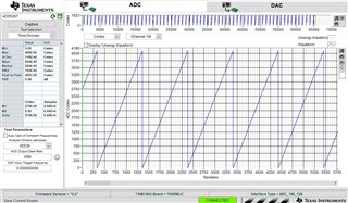
    I set up the ADS5287EVM in the lab with a sample clock of 12.5 MHz. Using the initialization sequence previously mentioned, I was able to output a ramp pattern (see attached image).

    Initialization Sequence:

    SPIWRITE    0x00    0x0001    // Software Reset (can alternatively be done with HW)

    SPIWRITE    0x01    0x0010    // Needed for AC coupled input

    SPIWRITE    0xE2    0x00C0    // Needed for AC coupled input

    SPIWRITE    0xE3    0x0060    // For Fs from 10 to 25 MHz

    Once initialized, a ramp pattern is generated by the register write:

    SPIWRITE    0x25    0x0040

    Previously, you had mentioned that your minimum sampling frequency could be 5 MHz, but that you are currently running at a sample rate of 12.5 MHz. This sampling frequency range indicates that you should write 0x0060 to register 0xE3 (please refer to the ADS5287 datasheet page 3). I notice in the code posted, that you are doing a 0x00A0 write to register 0xE3.  

    The first thing I checked was a write to powerdown. With a 5V input and a 12.5 MHz clock at 7 dBm, I observed that the current draw decreased just over 100mA, from 146 mA to 40 mA. Please start by verifying that the powerdown write behaves similarly on your end.

    Rob and I would still be happy to discuss how our newer parts may fit your application. Just let us know if you are interested and we can get a call set up.

    Regards, Amy

  • Hi Amy,

    Thanks for your efforts and the feedback on the startup.  I am really busy this week but I would like to discuss newer parts with you and Rob at some point next week if that works for you.  Let me know a date and time other than Monday that can work for you and Rob and I will make it work.  You can also call on my cell phone if you like 401-487-9323.

    Regarding your comments, we will try things out with the updated register writes and let you know how we make out.  Related to the sample rate info, do you know why there is a lower limit on the speed the device can run at.  It would be best if we could run it a 5MHz as I mentioned before.  If you could check it out and let me know if 5MHz sample rate operation CAN work OR is 10MHz the absolute lowest we can go.

    Thanks again for the information and I look forward to speaking with you and Bob next week.

  • Hi Michael,

    The 10 MSPS to 65 MSPS sampling rate is the range over which the part was tested. We can’t guarantee part functionality outside of this range.

    A sampling rate of 5 MSPS falls in line with Precision ADC products (<=10 MSPS). You can do a quick search with your desired parameters to see if there is a part that would better fit your application.

    https://www.ti.com/data-converters/adc-circuit/precision-adcs/products.html#p593max=500;5000&sort=p593max;desc

    If you still have additional questions after looking at this page, please provide a good email address and we can set up a meeting. I sent you an E2E friend request so that you can message me directly.

    Regards, Amy