This thread has been locked.

If you have a related question, please click the "Ask a related question" button in the top right corner. The newly created question will be automatically linked to this question.

DAC8760: About change of datasheet

Guru 21045 points
Part Number: DAC8760

Hi Team,


The datasheet has changed from Revision C to D.

I understand that there are two changes to the recommended circuit:

-Additional 100-pF capacitor from CMP to GND

-Additional 10ohm series resistor from the analog supply to the device AVDD


If there is other change(additional) point, could you please let us know this point?


Currently, our circuit don’t have 100pF and 10ohm.

Could you please let us know your concern?


Regards,

Hide

  • Joe will provide a detailed answer when he is back in the office on the 3rd.

    Thanks,

    Paul

  • Hide-san,


    The 100-pF capacitor is only needed when larger capacitors were used from CMP to VOUT. For values CMP capacitances of 470 pF or lower, this extra 100-pF capacitance from CMP to GND is not needed. In some cases, an electrical fast transient with larger CMP capacitors could couple charge from VOUT to an internal node of the output amplifier through the CMP pin. This could cause damage to the device.

    The series resistance was added because fast ramps of the supply (~1nV/sec) could be destructive to the device. This fast ramp could be seen when the device is powered similar to hot-swapping supplies. Using a resistor would lower the in-rush current from this kind of event. Using a series resistance and a bypass capacitor would also slow the supply ramp of the device.

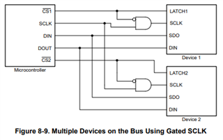
    The only other recommended change to the circuits would be for using multiple devices on an SPI compatible bus. We recommend that the SCLK be gated with the /CS. This way, the device does not receive SCLKs when the device is not active. This is shown in the datasheet on page 41 in Figure 8-9.


    Joseph Wu

  • Hide-san,

    Just a note about the fast ramp of the supply - I meant that a ramp of 1V/ns may be a problem (not 1nV/s).

    Joseph Wu

  • Hi Joseph-san,

    Thank you for the information.

    I greatly appreciate your cooperation.

    Regards,

    Hide

  • Hi Joseph-san,


    I have one more question.


    Currently, we use 1000pF for CMP to VOUT at our circuit.

    Because, 1000pF(1nF) is a recommended value in the datasheet.

    (So CMP to COUT capacitor more than 470pF.)


    Therefore, we would like to change from 1000pF to 470pF.

    What kind of spec evaluation should be done?

    (For example, settling time etc.)


    Regards,

    Hide

  • Hide-san,


    The CMP pin is connected to an internal node in the output amp for the voltage DAC. This is used for capacitive compensation for stability in the amp.

    If you change of the CMP capacitor from 1000 pF to 470 pf, there are only a couple things that I think you should look at. As you mentioned, settling time will change. This is shown in Figures 7-36 to 7-38. The other thing that changes is the ability to drive a load capacitance. With 1000 pF at the CMP pin, you would drive more load capacitance, but with 470pF you would get the result as shown in Figure 7-38.

    Note that if you kept the 1000 pF CMP capacitance, and added a 100 pF you still may be reducing the load capacitance drive anyway.


    Joseph Wu

  • Hi Joseph-san,

    Thank you for the detail information.

    Regards,

    Hide