Part Number: ADS8900BEVM-PDK
Other Parts Discussed in Thread: ADS8900B, , THS4551
I want to test the EVM board without PHI, meaning directly communicate with the ADC chip with a STM32 MCU.
I was told here (https://e2e.ti.com/support/data-converters-group/data-converters/f/data-converters-forum/1056122/ads1675ref-fast-adc-1msps-with-low-error-0-5mv/3913091?tisearch=e2e-sitesearch&keymatch=%20user%3A223776#3913091) that I need to apply power to DVDD and LDO_IN.
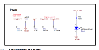
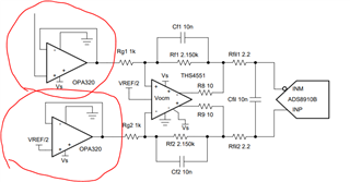
- According to the schematic, both power level should be 5.3V. Is it correct?
- Is there any requirement for the power supply for LDO_IN? I wonder if it is OK to draw power from power output pin from a STM32 G431 board.
- In the power schematic drawing, there are pings like TP12, 13, 14,15 and 16. How come there is no marking on the board.