This thread has been locked.

If you have a related question, please click the "Ask a related question" button in the top right corner. The newly created question will be automatically linked to this question.

ADS8363EVM BUSY

Other Parts Discussed in Thread: ADS8363EVM, ADS8363, MSP430F2013

Hi.

I come from Beijing and have an ADS8363EVM board. There are some problems about the busy time series. I configured the board as follows.

FCK=1MHZ;

VD was 5V;

VA was 5V;

RD connected CONVST;

CMA connected REF1; CMB connected REF2;

M0 was high; M1 was high; SDOB was high impedance;

The SDI data did not write to ADS8363EVM;

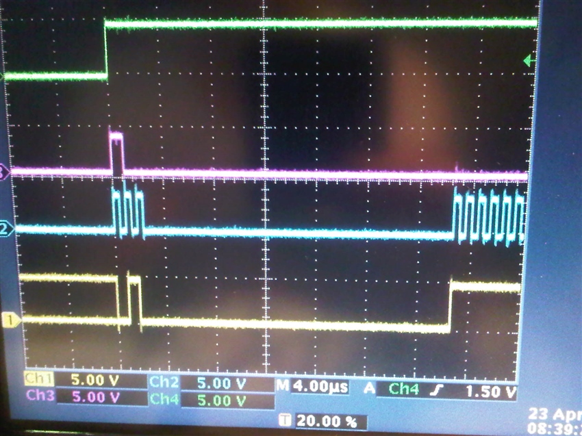
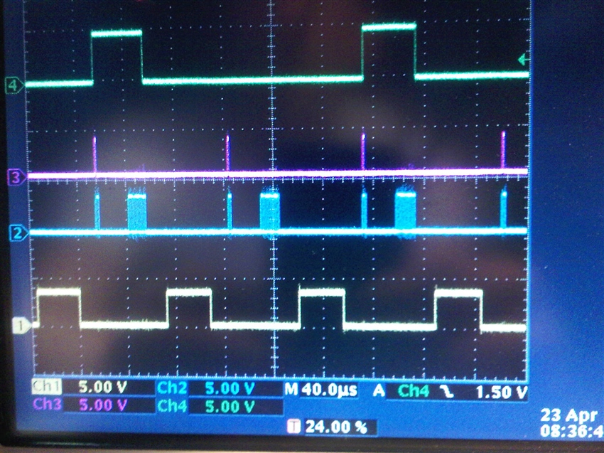
1\ SCK and CONVST time series(SCK was green line and CONVST was yellow line):

2\ RD and BUSY time series(RD was green line and BUSY was yellow line):

Could you explain what happened to the busy line?

Thank you very much!

Daisy

  • Hi Daisy,

    It looks like you have lost synchronization with the ADS8363.  In Mode IV, the CONVST has to be one SCLK wide.  Can you reduce the width of the combined RD+CONVST and see if that takes care of your communication issues?

  • Hi again Daisy,

    Here is an example of running the ADS8363 in Mode IV using an MSP430F2013 - perhaps an unconventional way to run the part, but it seems to be working.  The F2013 has the USI port which allows you to control the number of clocks per transfer.  I've set the device up to run one set of 3 clocks and a second set of 16.  I've also used SIMO as the input strobe for RD+CONVST by writing 0x8000 into the shift register.  What that does is shown below:


    The SIMO output connected to the RD+CONVST input (by writing 0x8000) puts a logic high on the combination of those two pins that is one clock cycle wide.  This starts the conversion process and the second two clock cycles hold the channel ID bits.  In the code, I simply store the two bit result in a variable called CHID.  From there, a second series of 16 clocks is generated by putting 0x0000 into the shift register - the SOMI pin of the F2013 captures the conversion result during this phase.  The traces above are (from the top) BUSY, RD+CONVST, SCLK and SDO - the channel ID bits in this instance are '10', indicating the data to follow is from channel A1.  The screen capture below shows the overall cycle.  You will note that the BUSY is only going high with every other application of the CONVST pulse.


    In the sequence above, the top trace is BUSY, followed by RD+CONVST, SCLK and finally the /CS input.  Let me know if this helps - I've attached the code for the MSP430F2013 as well - this was run on the free version of the IAR Embedded Workbench software along with the EZ430-F2013 hardware.

  • Tom

    Thank you very much. Your pictures are helpful  to me. Could you please provide the sequence for SDI?  

    In your picture, it was a long time from the set of 3 clocks to the set of 16 clocks.  Why?


  • Hi Daisy,

    As I mentioned in the previous post, the way I was running the ADS8363 was a bit 'unconventional' in that I was using the MSP430F2013 as the host processor.  The delay between the first three clocks and the second sixteen is caused by the USI peripheral.  I was actually using the MOSI as the RD+CONVST input, so getting you a true SDI transfer is not possible with that processor.

    Here is another screen shot that is more consistent with the ADS8363 capabilities:

    This is a simple write to the part to enable the DAC.

  • Thank you!

    I will try it.

    Maybe I ignord something.

    Is +5V logic necessary, if VDD is 5V, and ADS8363 is used on mode IV?  FT2232 is +3.3V logic.


    Best wishes

    Daisy

  • Hi Daisy,

    My pleasure!  The ADS8363 has two supply rails - AVdd and DVdd.  You can connect DVdd to the same 3.3V supply you are using for the FTDI device.  The AVdd rail can be 5V with the digital rail at 3.3 - no worries there.

  • Hi Daisy,

    Did you ever get this working correctly?