This thread has been locked.

If you have a related question, please click the "Ask a related question" button in the top right corner. The newly created question will be automatically linked to this question.

ADS1247: Can anyone say (by photo) is this ADS1247 fake or not

Part Number: ADS1247
Other Parts Discussed in Thread: ADS1248

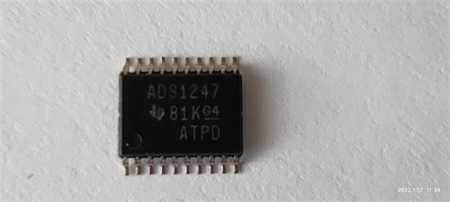
Hello! We have some ADS1247 that don't work correcty in our devices. Such IC have Reference value 2.038 (the lowest in datasheet but applicable) V instead of typical 2.047 - 2.049 and some strange (non typical) marking of TI on the left side. I have two pictures: top and bottom.   

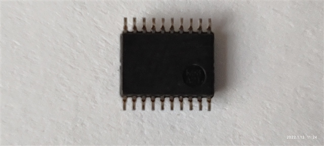
Another one. There is bad ADC marked by "?". There is also good ADC marked by "OK"/

  • Hi Youry,

    Both devices you have shown in the second image have topside markings that are in our system, so they appear to be real devices.

    Can you share where you purchased these items from? If you would like to share privately, please click on my name and select "Request Friendship", which will allow us to share messages offline.

    -Bryan

  • Ok, now I do think that the devices are all OK. More, I have PCB that contains ADS1247 having 2.048 reference and an application doesn't work correctly. I have some questions:

    1. Can ADS1247 work with high impedance signal source? For example, our application has voltage devider that consist of two resistor of 110 k (upper) and 10 k (lower). Input voltage may be up to 20 V, so output may be up to 20 / 11 (devider ratio) that is 1.81 V. Of course, we have PGA = 1.

    2. What is the maximum impulse current that can be sink (or sourced) by ADC in converting mode? I suppose that some current spikes with high impedance can cause additional error signal.

  • Hi Youry,

    I am glad the original issue has been resolved without too much effort.

    The effective input impedance is shown in Table 8 in the ADS1247 datasheet. As you can see from that table, the input impedance is on the order of 100s of MΩ at the fastest data rate (and only increases as data rate decreases). So a 10k resistor in parallel should not cause a significant error. You can calculate the theoretical error using these values if you choose.

    Regarding your second question: I am not sure what you mean here. Are you asking what is the maximum current you can apply to the ADC inputs? Or what is the maximum current the ADC will draw while converting? It sounds like it is a mix of those two questions, so any clarification would help.

    -Bryan

  • Hi Bryan,

    thank you very much for your feedback :-)

    About the second question: yes, I meant the maximum current that the ADC vill draw while converting. I suppose, that if the current is high it will make the voltage drop on 110 kOhm devider. So it can cause measurement error. Unfortunately I can't find such information in the datasheet. I could be inatintive while reading the doc:-( 

  • Hi Youry.

    We don't specify the maximum power dissipation for the ADS1247 as there are many different device features and settings.  You can get a basic idea from the electrical characteristics power supply data shown on page 10 of the ADS1248 datasheet.  These values are only shown as typical and do not include the use of the IDACs.

    I am not sure why the power draw from the ADC would affect the input current dramatically. You can see from the same table that the input current does have some dependency on sample rate, but it is still within the single-digit nA range. So I am still unclear why this would affect the measurement accuracy.

    -Bryan

  • Hi Bryan! Thank you very much for clarification! I think this issue is answered now. The ADCs aren't fake)