This thread has been locked.
If you have a related question, please click the "Ask a related question" button in the top right corner. The newly created question will be automatically linked to this question.
Hi Experts,
May I ask if you can please provide the schematic of the ADS4222EVM (LVDS) board?
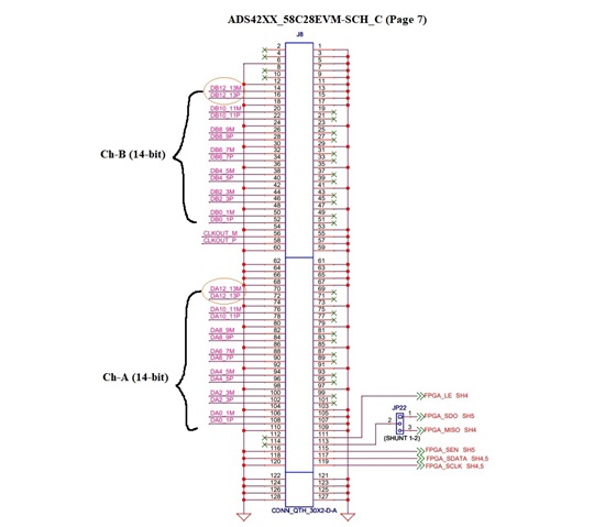
Our customer downloaded the schematic of ADS4222EVM from here (ADS42XX_58C28EVM DesignPkg (Rev. B) — SLAC459B.ZIP (6548 KB) ). Customer said, the pinout of "U2" (in the previous link) does not match with ADS4222 specified in the datasheet (please compare ADS4222 package on page 6 of the datasheet with "U2" in ADS42XX_58C28EVM DesignPkg (Rev. B)).
As I have also check, it seems that the DBxx and DAxx creates the difference between pin names. I am also wondering why it was not labeled with the same pin names as the datasheet of ADS4222. Kindly confirm. Otherwise, please advise. Thank you so much.
Kind regards,
Gerald
Hi Gerald,
The ADS42XX family consists of several parts, so the pinouts in the schematic found on the EVM page are named generically. Please advise to follow the pinout specific to the ADS4222 as found in the device specific datasheet.
Regards, Amy
Hi Amy,
Thanks for your response and I apologize for re-opening the thread. I just want to confirm, does it mean we should assume that pins 14,16, 70, and 72 of J8 are not used for ADS4222EVM board because ADS4222EVM is a 12-bit ADC (please see the attached photo). Is that right?
Looking forward to hearing from you and thank you so much for helping us understand.
Kind regards,
Gerald
Hi Gerald,
The generic naming does make things a bit harder to see. It looks like pins 58, 59 and pins 38,39 are NC pins. Pins 60,61 are DB0 and DB1 on the generic schematic, but are NC on the ADS4222, meaning that DB0_1M and DB0_1P are not used. Similarly, Pins 40,41 are DA0 and DA1 on the generic schematic, but are NC on the ADS4222, meaning that DA0_1M and DA0_1P are not used.
Hope this helps clarify.
Regards, Amy