According to the datasheet:
"7.3.4 Power-On Reset
The power-on reset circuit controls the output voltage during power-up. Upon application of power, the DAC
register is filled with zeros and the output voltage is 0 V and remains there until a valid write sequence is made to
the DAC."
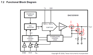
How exactly is this 0V achieved? Looking at the Functional Block Diagram, is sw-1 closed while sw-2 & sw-3 are open and the 0V is from the circuitry to the buffer out? OR sw-1 is open while sw-2 or sw-3 is closed to GND to achieve 0V? If this is the case then which is it, the 5K to GND or 100K to GND for 0V output?
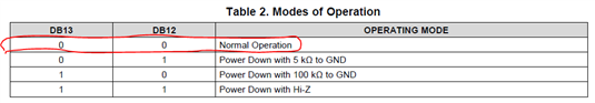
From the datasheet it also says "...the DAC register is filled with zeros.." which means that registers DB12 & DB13 are also zeros which is "Normal Operation", and this makes me think that the 0V is achieved through the circuitry to the buffer out instead of 5k or 100k to GND. Although I'm hoping that I'm wrong.
The reason for this question is because I'm trying to figure out if I can put a pull-up resistor on the output for my voltage divider as a fail-safe measure in the event of a power cycle reset and cannot program the IC in time, there will still be an output voltage. I'm hoping that this 0V output during Power-On Reset is achieved through the 100k to GND.