We are using an AFE58JD32ZBV in our design with the JESD interface. I am noticing something that I cannot explain and am looking for help.
The following figure is Figure 81 in the datasheet. First, can anyone explain the dotted vs solid line of TX_TRIGD? That may explain what I am seeing. I am not sure.
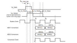
What I am seeing is that the even/odd conversion seems to be 1 system clock cycle delayed from what this diagram is showing. We have an external 4-to-1 mux (yielding a total of 128 ADC channels). For my experiment, I am connecting the output of the 4-to-1 mux to AIN16 of the AFE58JD32. I have 1 of the 4 mux inputs connected to 200mV and the other 3 connected to GND. If I switch the mux control lines at the neg clock edge of system clock where the conversion starts, the 200mV signal shows up split across 2 of the 4 mux channels. That mux switch timing should allow for the mux to switch and the AIN16 input sampling cap to be fully charged on the next clock cycle before the conversion on the following clock cycle. See the diagram below, also from the datasheet.
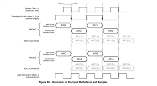
Here is a diagram that illustrates how we are switching the external mux control lines relative to the expected sample and conversion window.
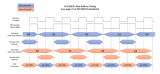
What I have discovered is that when I delay the mux control line switching by 1 system clock cycle, then the 200mV only shows up on just 1 of the 4 muxed channels as expected. However, I cannot explain this and would like to understand why this is the case.
Some other things:
1) I have tried using a TX_TRIG that is a half system clock cycle (falling to rising) in duration like the diagram above shows, and I have tried a full cycle TX_TRIG (falling to falling). Both yield the same behavior.
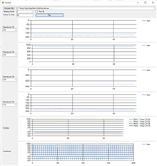
2) 200mV erroneously split across two of the 4 muxed channels:
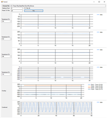
3) 200mV showing up on 1 of the 4 channels as expected, but only after 1-cycle delaying the mux control lines.
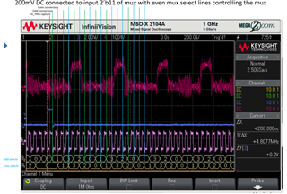
4) Scope picture showing TX_TRIG (ch3) and the mux select lines (B2 is odd, B1 is even) relative to ADC_CLK. You can also see the analog signal changing with even mux select lines. Please disregard the noise on the analog signal.
Thank you!

