This thread has been locked.

If you have a related question, please click the "Ask a related question" button in the top right corner. The newly created question will be automatically linked to this question.

ADS42LB69: RF Input impedance of datasheet circuit

Part Number: ADS42LB69

Hello,

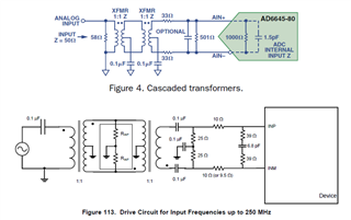
Just a question about the latest version of the ADS42LB69 datasheet.  On page 62, figure 113, this is a circuit listed as "Drive Circuit for Input Frequencies up to 250 MHz".  I searched around the forum and could not fine it but has anyone from TI ever posted measured data of the input circuit?  I want to  know what the input VSWR would likely be for such a wideband input with listed components.  Based on the EVM BOM, the xfmrs look to be Coilcraft WBC1-1TL.  In any case I would like to see what to expect with the circuit as listed.  

thanks

dennis brown

  • Dennis,

    We do not have VSWR data for this input.

    Regards,

    Jim 

  • Hi Dennis,

    The converter has a switched capacitor internal frontend. This means there is not buffered input and the impedance is time-varying.

    This is captured in the datasheet on the previous page, 61.

    If you would like a plot of the VSWR on the current EVM. I am happy to take this measurement for you. Just give me a few days.

    Please let me know if this will help.

    Regards,

    Rob

  • Hi Rob,

    Yes, on the data sheet the impedance of the ADC input is modeled but what I wanted to know is the impedance looking into the circuit, at that input voltage source (before that first series 0.1uF top of page 62).  If the connector on the EVM board was a SMA or whatever, at that point.  How good is the match up to 125M or 250M?

    Reason I am asking is that in my simulations/measurements show the transformers are very influential here.  We are laying a board out using this ADS42LB69 ADC and making changes here but the xfmrs are pretty touchy.  Right now it looks like the coilcraft WBC1-1TL is the best choice but I don't want to deviate much if it works.

    I am seeing an input VSWR going outside of a 1.5:1 VSWR circle.  I just was not sure what to expect.  I would like to see a dot at 50ohms for wideband but that won't happen due to the xfmr reactances not behaving.  They are not perfect.

    dennis brown

  • The input bandwidth I am going for is 100k - 125MHz but the low freq end has some give and may be closer to 1MHz.  

  • Hi Dennis,

    Yes, I understand the measurement request. I will measure from the SMA inward to include the frontend within the freq range specified above.

    Stay tuned.....

    Thanks,
    Rob

  • Rob,

    Thanks for this.  You have no idea how much I do appreciate this info.

    Technically this resolves the issue/question I asked about.

    However, as for a last comment, what can I do to create a better wideband match here?  This is out of the scope of my main question so I could start a new thread going after this aspect. 

    dennis brown  

  • Hi Dennis,

    Essentialy, we need to create different match here.

    What I measured was the default on the EVM. I can look at modifying the EVM to use the same circuit, on page 62 of the datasheet.

    Let me try that next and I will send you another round of files.

    Regards,

    Rob

  • Hi Dennis,

    I did some modifications per the DS recommendations on page 62. Figure 113 and 114, for freqs up to 250MHz and greater than 250MHz respectively.

    I don't see much change in the VSWR.

    It might be better to start with the application bandwidth you are using?

    I see its up to125MHz, but what is the low end BW frequency? 

    Then, can you tell me what passband flatness you are trying to design to? for example, 1MHz to 125MHz at -2dB across the band?

    Please let me know and I can research a better match with appropriate rolloff.

    Thanks,

    Rob

  • Hi Rob,

    Some specs I am looking for to meet:

    Freq range: 1 - 125MHz (be nice to hit 100kHz but I will sacrifice LF a bit)

    Input VSWR: < 1.5:1 across the band (but might not be a realistic goal)

    Flatness: i am ok with 2dB across the band as a starting point

    I think max Vin is something like 2Vpp, or +10dBm for power so no real changes there.  

    dennis brown

  • Hi Dennis,

    Noted, I will work on this and get back to you. Please give me a few days.

    Regards,

    Rob

  • PS - right now the frontend is about -7dB loss across your band. Per the datasheet configurations.

  • Rob,

    No problem about time needed.

    And before you ask, i am not considering going to a FDA at the input.  Want to keep this passive as adding an active device creates other problems.

    As for as passband loss goes, balancing between that and impedance match is a challenge.

    dennis brown

  • Hi Dennis,

    I don't plan to push you into an active design.

    Need to create a frontend that we resonate out the internal input network to help with dial in the passband flatness and rolloff.

    This will automatically translate to better VSWR.

    Regards,

    Rob

  • Hi Rob,

    Just a question: What is the correct way to connect dual transformers up?  TI datasheet says one thing and your background in this type of thing shows differences.  Maybe it does not matter with a 1:1 xfmr but this is what I am asking.  TI has back to back center tap connections, the other way in just two xfmrs in series.  

    dennis brown

  • HI Dennis,

    Do you mean on the TI figure, the Rint resistor connections or the 25ohm center tap connections?

    One reason why the ADI cascaded transformer circuit is different from the TI version, is that the TI ADC is a unbuffered and the ADI ADC is buffer. Which means each of these analog inputs have different criteria in order to make them work sufficiently.

    Regards,

    Rob

  • PS -  I will work on your other design this week. We had some bad weather here in Dallas and I haven't been in the lab for a few days.

    Regards,

    Rob

  • Hi Rob,

    Thanks for the reply. 

    Not trying to be difficult here but the TI ADS42LB69 datasheet says it is buffered.  

    I am just trying to understand the differences here.

    dennis brown

  • Hi Dennis,

    My bad, I saw the CRC filter on the front there, and made the wrong assumption.

    In terms of the termination style, I cannot comment directly, as this part, ADC42LB69, has some history that I am not currently privy too.

    Anyway, I wouldn't agree with the double termination around the transformer, as this tends to load down the analog input. ie - more loss.

    When I look at the EVM directly, the Rint resistors are not installed. This maybe just another termination option, in case a user would plan to remove the second transformer and want to terminate close to the first transformer.

    In the end, both schematic circuits would work and terminate for a 50ohm source to drive it.

    Hope that helps.

    Regards,

    Rob

  • Hi Rob,

    Thanks for the update.  I am currently in layout with this area of circuit and I am using two xfmrs but the center taps are not facing each other, in a true cascade I suppose (like the ADI AD6645-80 above).  I have two simulations in ADS, one configured with CT's facing each other and the other with CT's not facing each other and I really don't see a difference in terms of impedance matching.  Yes, I get slightly different values in some resistors but they are pretty similar. I do have the ADC front end modeled as a load impedance based on the data sheet using ADS Z1P black box.  I would be willing to send these to you but not via the forum here.  Contact me via email/PM if you want to see this. 

    In any case I was going to use a kitchen sink approach where I have those Rint resistors but they are not populated.  I will also say that I did a lumped element model for my transformer, that being the wild card.  I tried to match it up with coilcraft's s-parameter version (too bad their models don't include the CT).  Any higher of a freq would be a problem for the design but I think my model is good enough for the intended bandwidth.  

    dennis brown

  • Hi Dennis,

    Thank you for all the details. There are a lot more details to uncover here in the simulations. A lumped element model is a good approach. But in the end, there will always be some tweaking of the network due to your specific layout, etc. So I tend to use a more practical approach.

    Which transformer are you planning to go with? Are both transformers the same part number too, correct?

    Thanks,

    Rob

  • Rob,

    I am sticking with coilcraft WBC1-1TL.  And yes, my xfmr model is ok but nothing beats a real device and testing.  Both xfmrs are the same.  I have built this up on my own proto boards and can get decent correlation between bench and simulation.  Simulation gives guidance and a nice optimizer but real h/w matters more.  Simulation did point me in the direction of which components were very influential so I know what to tweak.  If you decide to post a circuit then that would be great.  I was able to use normal R,L,C, parts and not go down the road of ferrite beads of any kind.  I will say that my experience with ferrite beads is pretty limited and not sure how to tell when to use them.  In any case I was able to hit my intended VSWR except at low freq but that seems more of a problem with xfmr characteristics.

    dennis brown

  • Hi Dennis,

    If you want to send your RLC network over, I can use that as a starting point.

    If you are uncomfortable with that, I can email you.

    Please let me know.

    Thx,

    Rob

  • Rob

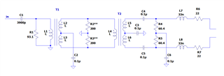
    I have no problem submitting my almost final circuit here.  There may be circuit changes like resistors values once a board is available.    

    I was not willing to post my ADS file where all the effort was.  

    maybe you will find something wrong here.  Note that R2, R3 are no pops but pads will be available.

    dennis brown

  • This circuit is nothing more than what I have collected from several app notes so it's not proprietary in that respect. 

  • Hi Dennis,

    The frontend design you implemented, looks great. We soldered up your design on the evaluation board and the "match" looks much better at 120MHz at first glance using the VNA.

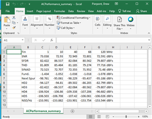
    We will post the collected data on Monday. I want to verify AC performance as well, SNR/SFDR/etc. to make sure nothing has gone amiss.

    Regards,

    Rob

  • Hi Dennis,

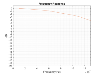
    I've enclosed the VSWR plot, passband flatness and AC Performance summary. Additionally, I've provided a zipped folder with those and full AC performance data in excel and screenshots for visual convenience.

    Please let us know if there is anything else you need.

    LB69_data.zip

  • Thanks for the updates.  I am glad to see this has worked out.  Since there was no other comments about any negatives with my posted circuit I am going ahead and use the design as posted.

    I don't know how the freq response compares to other versions of similar circuits so I take it as being acceptable to use.


    dennis brown