Hello!
I'm doing a project where I need to connect a high speed ADC(ADC12DJ5200RFEVM) to an FPGA(VCU118). The system could be like this:
ADC -> (FMC) -> FPGA.
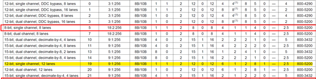
I need to transfer 12bit wide data sampled by ADC from channel A at 10Gsps from ADC to FPGA, so I choose to use JMOD19 mode.
ADC has link A and link B, and they correspond to BANK121(link A), BANK122(link A), BANK125(link B) and BANK126(link B) on VCU118. In addition, BANK 121 and BANK 122 in the SLR0 of VU9P, and BANK 125 and BANK 126 in the SLR1 of VU9P. The SLR is SLR(Super Logic Region) in VU9P.
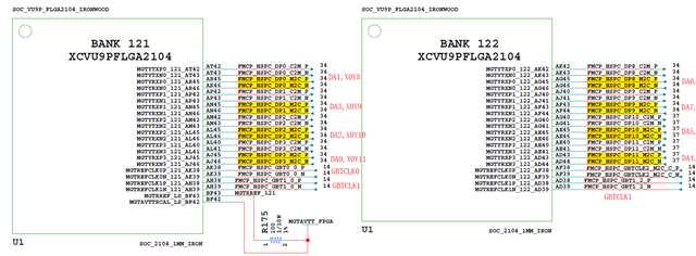
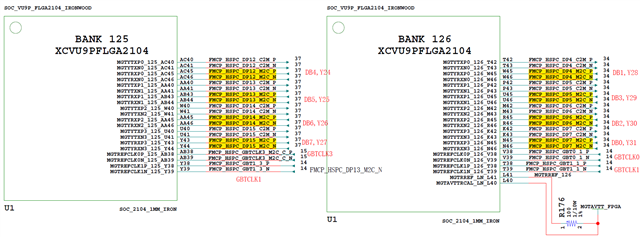
In each link, I use two jesd204 PHY cores and one jesd204 core, and the two PHY cores share a REFCLK (reference clock).
Results when debugging, the result received from link a is correct. On the contrary, the result received from link B is wrong.
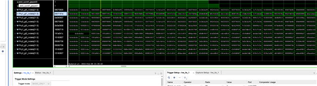
I found that the alignment of lines is K28 5, there is no difference between the two, but in the ILAS stage, the data output by the two link PHY cores is different.
In the ILAS stage, the first multi frame should be an incremental counter. The PHY core output (py0_gt0_rxdata) of link a is correct and the PHY core output (py1_gt1_rxdata) of link B is wrong.