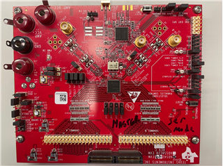
Part Number: ADS4249EVM
I have powered up the board with +5V across J10 and J12.
I am sending a clock signal (0.5V rms sine wave) into J19
by my calculations that gives a 1.5 V sine wave to pins 26 and 27 of the ADC as described in Table 7.3 of the datasheet.
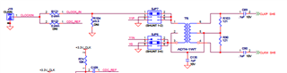
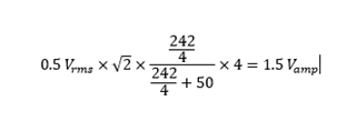
I should expect to see a clock signal coming out of the ADC at pins 56 and 57, right?
well I don't get any signal there. I am measuring with a probe at pins 5 and 6 of RN8
Is there some setting I need to change using the GUI?
Is my board defective?
Thank you.