This thread has been locked.

If you have a related question, please click the "Ask a related question" button in the top right corner. The newly created question will be automatically linked to this question.

TSW1265EVM: DDR TIME_OUT_ERROR !!!

Part Number: TSW1265EVM
Other Parts Discussed in Thread: ADS52J90EVM, , ADS52J90

Hi,

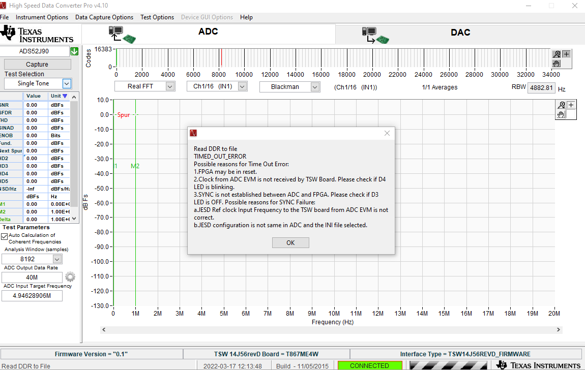
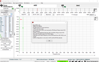
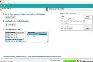
We are testing ADS52J90EVM and we used TSW1265EVM to capture the output data.

but every time we try we get an error: 

Read DDR to file 

TIME_OUT_ERROR

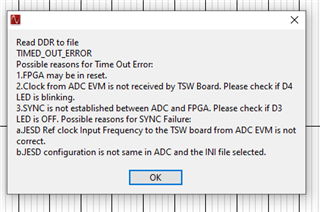
I have checked D4 is not blinking (OFF)

D3 is not OFF (ON)

and the input  CLK ADS52J90EVM  ,J75(LMK _CLKIN1 )is 40/60MHz.

Could you please check this issue?

Best Regards,

Bhaaeddin

  • Hi,

    the TSW1265 is an RF receiver EVM. It is not an FPGA capture EVM. I am routing your request to TI medical team for support of the ADS52J90 EVM

  • Hi,
    Any updates regarding this case?

    BR/

    Bhaaeddin

  • Hi Bhaaeddin,

    The ADS52J90EVM will not work with TSW1265 EVM due to the following reasons:

    1. TSW1265 is not a data capture solution as it does not have any FPGA, in fact it itself uses TSW1400 as a pattern capture and generation card for quick evaluation

    2. The firmware is not compatible to TSW1265

    The ADS52J90EVM will need either TSW1400 for LVDS data capture and TSW14J56 for JESD data capture.

    Thanks & regards,
    Abhishek

  • Hi Abhishek,
    Sorry, Our board is TSW14J56 (JESD data capture),

  • Hi Bhaaeddin,

    Let me try to replicate the same in the lab and I will get back with possible solution by tomorrow.

    Regards,

    Abhishek

  • Hi Bhaaeddin,

    Sometimes the power supply current limit causes such issues, can you provide 2 independent power supplies to the EVM and the TSW card, set the current limit to max (say 3 A both) and check if it works.

    Next, after applying the supply and connecting the clock source, and setting up the LMK, can you probe if you are getting the required clock on  TP8 and  TP 10. These are ADC_CLKP and ADC_CLKM. Also check if the FPGA clock is getting generated or not by probing TP4 and TP5.

    If above doesn't work 

    Can you check the following:

    1. Make sure that jumper settings are such a way that AFE uses 40 Mhz crystal clock.

    2. Undock the TSW card. Connect the power supply to AFE board and press the hardware RESET button on EVM.

    3.  Probe the device FCLK on the test point available 

    4. The device will be in 12x serialization mode and will be in LVDS mode. You should observe 40 MHz square when probed.

    If this simple test fails, we can confirm that the board is has some issue. 

    Thanks & regards,

    Abhishek

  • Hi Abhishek,

    It works, but do you know how to find the frequency of the captured signal in GUI,

    1-I converted the x-axis to time and calculate the frequency,but it is not correct (it is not the same frequency I have applied on SMA-ch1).

    2-What is the minimum frequency for the input analog (Ch1-Ch32)? below 10KHz the captured signal was destroyed!!

    Best Regards,

    Bhaaeddin

  • Hi Bhaaeddin,

    Are you asking about the sampling frequency? Or the signal frequency.

    Can you share the details of the settings or mode you are running on the device ? i.e 32 ch mode or 16 ch mode, what is your PLL mode? etc.

    Regards,

    Abhishek 

  • Hi Abhishek,

    I am asking about the signal frequency (analog input SMA Ch1).

    I am using :

    32 Channel mode 14bit (ADS52J90_32ch_SINE_4L_16x_14b_GBLCLKDIV1_FSDIV4_SYSREFDIV32_20x),

    250MHz applied LMK_CLKIN (J75).

    1-Input analog signal to channel 1 : freq 35kHz ,Amp 240mVpp ,offset 0

    The amplitude of the signal is not right, is there any limitation for the minimum analog input frequency 

    2-Input analog signal to channel 1 : freq 3MHz ,Amp 240mVpp ,offset 0

    We noticed that the sampling frequency was around 30MSPS only.do you know how to achieve a high sampling rate (65MSPS) with 32 inputs?

  • Hi Bhaaeddin,

    Thanks for sharing the waveforms. I understood your concern.

    Regarding your queries:

    1-Input analog signal to channel 1 : freq 35kHz ,Amp 240mVpp ,offset 0

    The amplitude of the signal is not right, is there any limitation for the minimum analog input frequency 

    TI: There is no lower limit on the input frequency, from the specification sheet the frequency range is 0-70 MHz.

    About the amplitude, can you check the input termination in the board, by default is should be 50 ohm differential. You can verify if it mounted or not. Also, check if similar observation is happening on other channels as well.

    I noticed that your sine waveform has a lot of glitches, I don't understand why it is coming, can you check if it is coming from the source itself? You can probe the input waveform without connecting it to the SMA channel. Next, you can compare the same at the input of the device at some test point whichever is available.

    Or, it may be coming from the Digital HPF, can you check your settings if you are using digital high pass filter?

    2-Input analog signal to channel 1 : freq 3MHz ,Amp 240mVpp ,offset 0

    We noticed that the sampling frequency was around 30MSPS only.do you know how to achieve a high sampling rate (65MSPS) with 32 inputs?

    TI: From the settings you are using, I think you are using 80x mode, and with 250 MHz LMK clk, so your ADC conversion rate will be 62.5MHz.

    For 32 Ch mode, your sampling speed will be 0.5 x 62.5 MHz that is, 31.25 MHz. as shown below in the datasheet, highlighted in yellow.

    This is because of the architecture of the ADC, there are 16 adc's which are interleaved to have 32 channels as an input. So each ADC will sample 2 channel at 65 Msps hence for 1 ADC channel the sampling frequency will be reduced by half.

    So, you can not achieve 65 Msps with 32 channels using ADS52J90 device.

    Thanks & regards,

    Abhishek

  • Hi Abhishek,

    Thanks for your reply,

    I have a question regarding the performance of the ADC (DC and AC).

    Do you know how to calculate the total error of the ADC (32 Channel mode 14bit (ADS52J90_32ch_SINE_4L_16x_14b_GBLCLKDIV1_FSDIV4_SYSREFDIV32_20x))?

    Best Regards,

    Bhaaeddin

  • Hi Bhaaeddin,

    Since the issue is not related to DDR timeout error.

    I request you to please raise you concern on a new thread and I will reply there. 

    Thanks & regards,

    Abhishek

  • Hi Abhishek,

    Could you please try to replicate this test in your lab, Input analog signal: freq 35kHz ,Amp 240mVpp ,offset 0?

    I am not using any HPF and the signal from the source is clean without any noise or glitchs.

    /Bhaaeddin

  • Hi Bhaeddin,

    I will check this issue with the design team and learn there feedback. If they could not get any reasonable explanation, I will try the test in the lab.

    Please allow me time to do that. Meanwhile can you post the same query on a separate thread. I am sorry but we have been asked to ensure different topics should be covered in a different thread. This helps our audit team to properly gauge the progress and other users who might have similar issue to reach to the thread.

    I am closing this thread as well.

    Thanks,

    Abhishek