This thread has been locked.

If you have a related question, please click the "Ask a related question" button in the top right corner. The newly created question will be automatically linked to this question.

ADS58C48: toggle pattern

Part Number: ADS58C48
Other Parts Discussed in Thread: LMK04828

Hi team,

Here is a question from one customer.

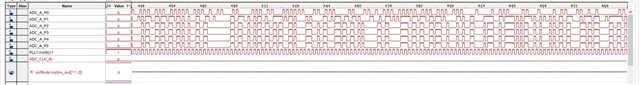
At present, it can communicate with ADS58C48 normally. The FPGA side is configured as DDR LVDS mode.

Set the ADC four channel output mode to outputs toggle pattern That is, the output is 10101010101 and 01010101010

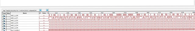
From the FPGA end, it can be seen that on A10, A8, A6 and A4, the data waveform conforms to the set output mode. However, this is not the data mode on the two LVDS lines A2 and A0. The same phenomenon exists in all four channels. Read the ADC register value after configuration, and the configuration value is consistent with the read value.

See the figure for details.

Other tests:

1. Configure output all zeros:

Configure Output all ones:

PLL1 in the figure is the input clock of ADC.

2. The input clock of ADC is the signal directly output by FPGA PLL frequency doubling. The frequency has tried 20M, 40M, 50M, 80M and 100M, and the amplitude is VPP = 2.5V. The clock output is correct, which has been measured and verified by oscilloscope.

3. The CM voltage is 0.95V.

4. This ADC peripheral design can work normally in other projects (the difference from this project is that the FPGA is replaced, but the pin definition and configuration are verified to be OK). The supply voltage, power consumption and configuration resistance of ADC have been measured and there is no problem.

5. The phenomenon is consistent after the PCB is rearranged.

What are the possible reasons for the above phenomenon? Could you give some troubleshooting suggestions

Best Regards,

Amy Luo

  • Hi Amy,

    the A2, A0 signal not toggling require further investigation

    Could you please advise the following signal net?

    Does ADC_A_P0 correspond to A0 LVDS bus, while ADC_A_P1 correspond to A2 LVDS bus?

    Regarding your statement below, I have a concern:

    2. The input clock of ADC is the signal directly output by FPGA PLL frequency doubling. The frequency has tried 20M, 40M, 50M, 80M and 100M, and the amplitude is VPP = 2.5V. The clock output is correct, which has been measured and verified by oscilloscope.

    The FPGA output clock typically has high jitter content, and will impact the ADC's SNR performance. For optimal ADC performance, please consider using TI's clock solution such as the LMK04828

  • Hi,

    Could you please also make sure digital_mode_1 is enabled? Thank you

  • Hi Kang,

    Register 42 is set to 0x08 and the read return value is 0x08.

    Does ADC_A_P0 correspond to A0 LVDS bus, while ADC_A_P1 correspond to A2 LVDS bus?

    Yes.

    Will the FPGA output clock cause the above phenomenon?

    In order to eliminate the problem of signal and clock phase, the phase of FPGA output clock is adjusted from - 40 ° to + 40 °, but it is not improved.

  • Hi Amy,

    We will have to check internally and get back to you on this. The ADS58C48 EVM are obsoleted so we will have to find some other way to validate this.

    -Kang

  • Hi Amy,

    We have located a ADS58C48 EVM. We will need to bring up the EVM first with the TSW1400 EVM and checkout the functionality, before also validating the data pattern mode. We will need to update you at a later time. thanks. 

  • Hello Kang,

    May I know if there is any update here

  • Hi Amy,

    No updates for now. We are working through the backlog and trying to bring up the TSW1400 + ADC58C48 EVM to get confirmation of the behavior. Thanks. 

  • Hi Amy,

    I was able to see all the bits with the LVDS toggle. Could the customer send over their configuration file for me to double check? Thank you

  • Hi Amy,

    Just FYI, the configuration that I used to capture all pattern is below:

    00	   x00
    25	   x00
    2B	   x00
    31	   x00
    37	   x00
    3D	   x00
    41	   x00
    42	   x08
    44	   x01
    45	   x00
    26	   x00
    28	   x40
    2D	   x00
    2E	   x40
    32	   x00
    34	   x40
    39	   x00
    3A	   x40
    BF	   x00
    C1	   x00
    C3	   x00
    C5	   x00
    CF	   x00
    EA	   x00
    3F	   x00
    40	   x00
    25	   x02
    2b	   x02
    31	   x02
    37	   x02


    I will go ahead and close this thread for now. Thank you.