This thread has been locked.

If you have a related question, please click the "Ask a related question" button in the top right corner. The newly created question will be automatically linked to this question.

DAC5672A: Interleave output signal behavior

Part Number: DAC5672A

Hello,

I would like you to confirm output behavior when we use interleave mode.
The data condition is when we input digital data for DAC A and DAC B one by one.

* According to datasheet, there is following section which explain behavior of interleave mode.

7.3.3 Single-Bus Interleaved Data Interface and Timing

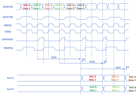
For this section, I understand as shown figure for above sentence.

1. When RESETIQ become high, DACCLKIQ from output of divider(div /2) become low. However, maintain "DAC A Data 1" by rising edge of WRTIQ. 

2. When RESETIQ become low, DACCLKIQ will rise up accompanying the rise of CLKIQ. After 4CLK(tlat) later + Pd, DAC A Data 1 and DAC B Data 1 will be output for each output port.

Same thing will continue for DAC data 2 and 3.

Then I have following questions.

Q1. Af first, is my above understanding and figure correct ?
Q2. If  Q1 is correct, is my understanding when user try to pair DAC output A and DAC output B, data rate should be CLKIQ / 2 even in the fastest case correct ?
Q3. If  Q1 is correct, I think that explanaion of "tlat" is strange.
Because, in case of interleave mode, when RESETIQ is high, DAC does NOT latch input data. CLK which latch for DAC is CLKIQ (In fact, CLKDACIQ)
Therefore I think that "WRT A/B" should be "CLKIQ or CLKDACIQ" in case of interleave mode. Could you please confirm about this and give me your feedback ?
  

BR,

  • Hello,

    Could you please give your feedback ?

    BR,

  • Ryuuichi

    This is a very old device and the designers are no longer available. I find the data sheet confusing as well. For the most part what you have is correct I think. The one item I do not think is correct is the data rate being CLKIQ/2. The timing diagram in the data sheet is showing the rising edge of this clock occurring with every sample. If the part was using both the rising edge and falling edge to latch the data, then the data would be twice the clock rate. 

    The data rate is twice the SELECTIQ rate.

    Regarding the latency, I think there is more internal logic used than what is shown in the block diagram. This would account for the 2 extra clock cycles of latency.

    A simple test for checking the interface would be to send all of the A data as 3FFF and all of the B data as 0000 and check the output of the two DAC's.

    Another would be to use two ramp patterns. One ascending and the other descending.

    Regards,

    Jim  

  • Hello Jim-san,

    Thank you for your reply.

    - 1 -

    --
    The one item I do not think is correct is the data rate being CLKIQ/2. The timing diagram in the data sheet is showing the rising edge of this clock occurring with every sample. If the part was using both the rising edge and falling edge to latch the data, then the data would be twice the clock rate. 
    --

    I mistook about following things.
    1.1. For my timing diagram which I previously post, frequency of SelectIQ is not correct. I changed same timing as data.
      
    1.2. I mistook the sentence for below.
    >when user try to pair DAC output A and DAC output B, data rate should be CLKIQ / 2 even in the fastest case
    What I would like you to confirm is data rate about changing from current data.


    Question : Could you please tell me whether following understaind is correct or not ?

    * When user try to pair DAC output A and DAC output B, changing data rate about changing from current data is SELECTIQ / 2 even in the fastest case.

    - 2 -
    I could not understand meaning of below.

    --
    Regarding the latency, I think there is more internal logic used than what is shown in the block diagram. This would account for the 2 extra clock cycles of latency.
    --

    Question : you mean that actual latency should be 6 clock (4 clock + 2clock) ?

    BR,

  • I believe it should be 4 clocks. To me, the description and the block diagram describe it as 2 clocks, so I was thinking 2clocks + 2clocks = 4 clocks total per the data sheet spec. 

  • Hello Jim-san,

    Which portion is following sentence described ? could you please show figure number of datasheet ?

    >the description and the block diagram describe it as 2 clocks, 

    BR,

  • Page 14: 

    "The edge-triggered flip-flops latch the A- and B-channel input words on the rising edge of the write input (WRTIQ). This data is presented to the Aand
    B-DAC latches on the following falling edge of the write inputs.

    I am guessing the DAC latch then latches the data on the next rising edge of CLKIQ.

  • Hello, Jim-san,

    Understood.
    Anyway, I understood that updated Iout data can be observed after 4clock later from the data was latched.

    BR,