Hi TI Technical Support Team,
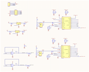
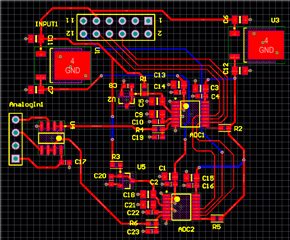
I have designed a small 4 layer board with 2 18bit 100kHz ADS8699 and I am planning to use it to read voltage and current values from the device under test. The top and bottom layer are used for routing signals. Internal planes are GND planes. The GND plane is solid and I did not make two seperate AGND and DGND. My voltage range is 0-5V range. I am converting current to voltage values and the voltage range corresponding to current values is between 1.5V and 3.5V. I have attached the schematic part of the ADC. I have following questions regarding the schematic.
1. I am not planning to use RVS, ALARM, RST pins of the device. Are the connections I made in the schematic correct, and also is there big issue in PCB layout?
2. I am using external 5V reference (ADR5045 0.2% accuracy) for the ADC. It is shunt reference. In the datasheet, the reference schematic uses series voltage reference REF5045. Does using shunt reference will make huge negative effect in reading the signals?
3. Is the filtering part for the ADC inputs correct?
Thank you very much for the help,
Ahmet