Hi, Im Juan Camilo.
I have the DAC5688 with this configuration:
| Register Address | Register Data |
| 0x01 | 0x09 |
| 0x02 | 0x60 |
| 0x03 | 0x00 |
| 0x04 | 0x00 |
| 0x05 | 0xB0 |
| 0x06 | 0x00 |
| 0x07 | 0x00 |
| 0x08 | 0x00 |
| 0x09 | 0x00 |
| 0x0A | 0x00 |
| 0x0B | 0x00 |
| 0x0C | 0xFF |
| 0x0D | 0xFF |
| 0x0F | 0x40 |
| 0x10 | 0x00 |
| 0x11 | 0x00 |
| 0x12 | 0x10 |
| 0x13 | 0x10 |
| 0x14 | 0x00 |
| 0x15 | 0x00 |
| 0x16 | 0x00 |
| 0x17 | 0x17 |
| 0x18 | 0x80 |
| 0x19 | 0x00 |
| 0x1A | 0x0E |
| 0x1B | 0xFF |
| 0x1C | 0x00 |
| 0x1D | 0x00 |
| 0x1E | 0x00 |
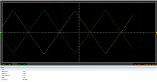
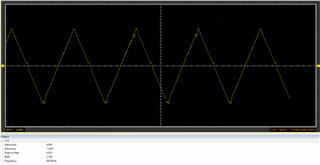
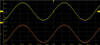
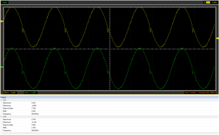
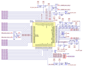
Im doing the steps in the section "RECOMMENDED STARTUP SEQUENCE" and after doing all this, the TXENABLE signal change from low to high. My clk1 is single ended (250 MHz) the CLK2 is differencial clock (500 MHz), the CLK1, DA and DB are provided by a FPGA and the serial interface, RESET, SYNC and TXENABLE are provided by a PIC.
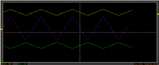
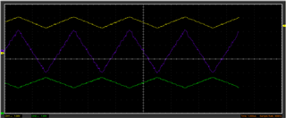
With the bit2 (inv_inclk) of CONFIG1 I can change the glitch from CH1 to CH2, when this bit is "0" the glitch is in CH2 and when is "1" the glitch change to CH1. I would like to know if I have the correct configuration on DAC5688 or I need to modify some registers.
Regards,
Juan Camilo Peña A.