This thread has been locked.

If you have a related question, please click the "Ask a related question" button in the top right corner. The newly created question will be automatically linked to this question.

TSW40RF82EVM: TSW40RF82EVM, TSW14J57EVM : How to set up for ADC

Part Number: TSW40RF82EVM

Hi.

I bought TSW14J57EVM and TSW40RF82EVM for ADC.

However, I don’t have any clues about how to use this two boards although I carefully read user’s guide.

Can you explain how to set up this boards for ADC step by step?


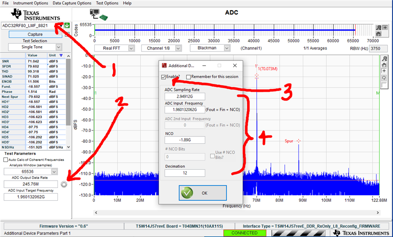
I want to set ADC clocking option as  LMK clock mode. :)

Thank you for sparing your precious time out of your busy schedule.

Best regards,

Seong

  • It's okay to recommend the easy-to-use ADC clocking options. (I can use external clock!)
    Thank you.

  • Hi Seong, welcome to the E2E forum.


    To begin evaluating TI ADC and/or DAC hardware, you will need to download software. The first one will be specific to the ADC/DAC EVM and is used to configure the device itself. You can find the download link to the TSW40RF82's GUI at the product page labeled as TSW40RF80EVM GUI Installer. https://www.ti.com/tool/TSW40RF82EVM#order-start-development 


    The second piece of software is a utility for the data capture board/pattern generator board (in this case, the TSW14J57EVM) called High Speed Data Converter Pro. This software is what you will use to view the captured data from the TSW14J57EVM FPGA. You can find the latest download at this link: https://www.ti.com/lit/zip/slwc107w 


    On the TSW40RF82 GUI, the steps for initial bring up of the ADC32RF45 is very fast. For fully onboard clocking, all you must do is choose the Load Default button at the home-screen or on the DAC38RF8x › Quick Start tab. This button will program the LMX2582, the LMK04828, and the ADC32RF45 to a default configuration. In this mode, the LMX2582 generates a 2949.12 MHz clock which supplies the LMK04828 for distribution to the ADC. The ADC32RF45 is programmed to use a decimation by 12 mode with the NCO set to 1.89GHz. This means the output data will show a window of 245.76 MHz (2949.12MHz / 12 ddc factor) wide of the data centered around the NCO value. 

    Open the High Speed Data Converter Pro software and connect to your TSW14J57EVM board:

    1. Choose the INI configuration file that is labeled as ADC32RF80_LMF_8821 
    2. Open the Additional Device Parameters icon
    3. Click the Enable? box to enable the fields
    4. Enter the information as I have shown below, these correspond to the default bring up settings.
    5. Press the OK button.
    6. Press the OK button for the popup that mentions the lane rate has changed. This is an informational text box only.
    7. Press the Capture button, unless there is a signal applied to input AIN, then you will see a noise floor.

    If you connect a signal generator set to 1.96013206G @ 0dBm into input AIN (connector J9), you will find a tone similar to below:

    If you want to operate the ADC32RF45 in bypass mode (bypassing the down-converter and decimation filter), you can change these settings in the TSW40RF80 GUI to enable this. Select the Low Level View tab and then click on the Open Configuration icon. In this menu, you will find various configuration files to program the ADC. If you would like to use external clocking, you will find these configuration files as well.

    I hope this helps to get you started evaluating these devices. Please let me know of any additional questions you may have.

    Regards, Chase