A related question is a question created from another question. When the related question is created, it will be automatically linked to the original question.
If you have a related question, please click the "Ask a related question" button in the top right corner. The newly created question will be automatically linked to this question.
I think a more correct way to explain this technique is to say that delay circuits (such as D flip-flop circuits) can help to avoid data transmission issues when the propagation delay is relatively large (i.e. close to one-half SCLK period). If there is relatively small propagation delay, this technique is not required.
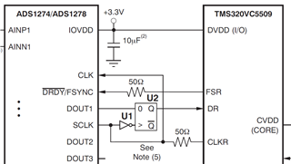
An example of this technique can be found in our ADS1278 data sheet:
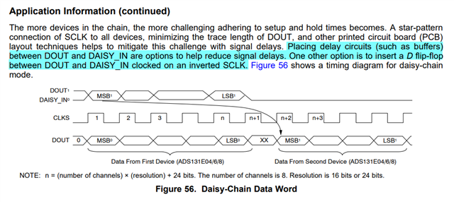
A large propagation delay can cause a problem when the SCLK edge for data capture (i.e. the trailing edge for ADS131E08) occurs before the next DOUT bit has transitioned and settled as seen by the MCU. This can result in the SCLK trailing edge capturing the previous old data rather than the settled new data. In that case, a D flip-flop with an inverted SCLK input can hold the data bit for an extra one-half SCLK period. The result is the MCU continues to use the SCLK trailing edge for data capture, but each bit is delayed by one full SCLK period, ensuring that the captured data is fully settled.
Again - I would not suggest implementing this technique unless it is proven the propagation delays in the system are causing problem.