This thread has been locked.

If you have a related question, please click the "Ask a related question" button in the top right corner. The newly created question will be automatically linked to this question.

ADS7853: SPI slow sampling rate

Genius 17905 points
Part Number: ADS7853


Hi Experts,

Good day. We have this query from Cx (he is using free email):

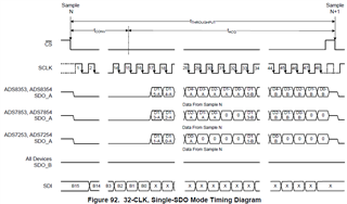
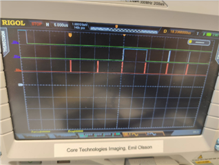
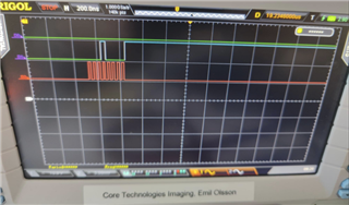
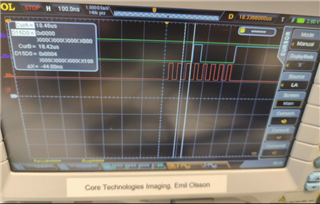
ADS7853: 14 Bits, 1 MSPS, but I am only receiving a 1kbps sampling rate when reading via SPI, do you have any advice on what could be the bottleneck? Do I need to use DMA to go faster than that?

Thank you.

Regards,
Archie A.

  • Hello Archie,

    Thank you for your post.

    The sampling rate is controlled by the CLOCK frequency and the timing of CONVST. The ADC switches from sample mode into hold mode on the rising edge of CONVST. Then the ADC begins converting the acquired voltage with the next CLOCK rising edge. The user has to manually set the CLOCK frequency and CONVST intervals to achieve the desired sampling rate.

    Regards,

    Ryan

  • Hi Ryan,

    Thanks for the guidance.

    Are you referring to the SPI clock? Cx have increased this speed significantly but no change has any influence.

    He is referring to the datasheet https://www.ti.com/lit/ds/symlink/ads7853.pdf but no registers/settings related to the "CONVST" that you mention, or the clock speed.

    Could you please refer us to where we can configure this or read more about these settings?

    Thank you!

    Regards,
    Archie A.

  • Hi Archie,

    My apologies - I misread the post as "ADS7863". 

    In ADS7853, there are two signals which control the overall ADC throughput: SCLK and CSn. The falling edge of CSn initiates the next conversion. During the first 16 SCLK periods, the conversion period takes place, after which the MSB and subsequent data bits are launched. There is a Data Launch Edge table pertaining to each data output mode.

    As soon as the conversion period completes, the acquisition period begins. The length of the acquisition period is controlled by the user and lasts until the next CSn falling edge.

    Best regards,

    Ryan

  • Hi Ryan,

    Thanks for the update. Just received fedback from Cx:

    He has experimented a lot with the SPI Clock frequency, but no matter how much he increase the frequency, the output read is stuck to around 1 kHz samples, i.e. around 0.001 - 0.002 seconds between each new value.

    Could you confirm if this is around the expected performance or if should be able to reach much higher? Their transactions are done by
    CS low
    16 bit transmit + 32 bit receive
    CS high.

    Thank you.

    Regards,
    Archie A.

  • Hi Archie,

    I do not understand the question. Both SCLK and CSn are signals provided from the MCU to the ADC. 

    Can you provide a scope or logic analyzer capture showing CSn, SCLK, and SDO_A? It sounds like the customer is using 32-CLK, Single SDO Mode (i.e. minimum 48 clocks per period). Is that correct? I'm expecting to see something similar to Figure 92:

    Regards,

    Ryan

  • Hello Ryan,

    Thanks for guiding. Below is the response from Cx:

    "Yes it is correct that I am using 32-CLK, Single SDO Mode (i.e. minimum 48 clocks per period).

    Below are the signals you requested in order (from above) CS, SDO_A, SCLK:

    Zoomed in on the first rising edge of SDO_A:

    So it looks like the ADC is correctly taking 16 clock signals input before the SDO outputs for 32 clock signals, as far as I can tell.

    This picture shows that there is around 44 ns between two clock rising edges, i.e. around 25MHz if I calculate correctly. 

    So with this configuration I am (in my MCU code) reading the ADC output and getting around 1000 complete values per second. (1 kHz). I am wondering if this is expected/reasonable performance of if I should be able to achieve much higher."

    For your assistance. Thank you.

    Regards,
    Archie A.

  • Hi Archie,

    Jumping in here since Ryan is out of office for a few days and will be back Tuesday 5/3. 

    Taking a look at your scope shots, I am unsure of the time/div in the first picture since it is a bit blurry. Is it 5us/div? Can you clarify? It would also be helpful if you can clarify what the frequency of the CS pin (CS Falling edge to CS falling edge) is. If you want 1MSPS, then CS falling edge to CS falling edge needs to be 1/throughput or 1/(1MHz) which is 1us. 

    Another point I would like to check is why there are intervals of SCLK. Can a constant SCLK be provided? Data should come out much faster with a constant SCLK since data out is dependent on the number of SCLK cycles. 


    Regards,
    Aaron Estrada

  • Hello Aaron,

    Sorry for the delayed response as Cx just updated after multiple attempts.

    Your previous guide made us realize some steps that can take to increase performance and that we have a misunderstanding around the actual sample rate trying to achieve.

    Requested to close this post since they need some time for further testing. Thanks a lot for your help.

    Regards,
    Archie A.