This thread has been locked.

If you have a related question, please click the "Ask a related question" button in the top right corner. The newly created question will be automatically linked to this question.

ADS9120: BQ: Each pin condition, and Data output

Part Number: ADS9120

Dear TI Community,

I'm very sorry for the really basic question.
Please teach me about ADS9120.


I designed circuit as shown on the next-figure.
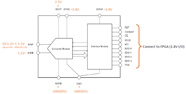
I think as follows:

The ADC full scale is defined by VREFP / M.
  -> In this case, the range from 0 to 2.5V.
ADC CODE 0000 is specified by AINM voltage.
  -> In this case, 1.2V.

Is this understanding correct?


In this case, I think that the data can be read as shown in the figure below.
Is this understanding correct?


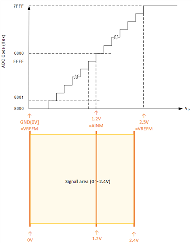
In the case of the configuration, I assume that there is a non-linearity region near 0V.
Is linearity around 0V guaranteed for this device?
If not guaranteed, how much voltage should be considered for non-linearity near 0V?


Thank you for your cooperation,

Tanigawa

  • Hello Tanigawa-san,

    First, welcome to the TI E2E community!

    In the case of the ADS9120, the input is differential, so the voltage that is converted is always the difference between the analog inputs.

    Here are a few examples of different DC input voltage levels and the expected code (assuming Vref=2.5V):

    0V differential input

    AINP=1.25V (with respect to GND)

    AINN=1.25V (with respect to GND)

    Vdiff=(AINP-AINN)=0V.

    Output Code (decimal) = [Vdiff/(2*Vref)]*2^16 = 0

    Output Code (HEX) = 0x0000h

    +1V differential input

    AINP=1.75V (with respect to GND)

    AINN=0.75V (with respect to GND)

    Vdiff=(AINP-AINN)=1V.

    Output Code (decimal) = [Vdiff/(2*Vref)]*2^16 = 13107

    Output Code (HEX) = 0x3333h

    -1V differential input

    AINP=0.75V (with respect to GND)

    AINN=1.75V (with respect to GND)

    Vdiff=(AINP-AINN)=-1V.

    Output Code (decimal) = [Vdiff/(2*Vref)]*2^16 = -13107

    Output Code (HEX) = 0xCCCDh (2's complement)

    If you notice in my above examples, the average voltage of the two analog inputs (AINP, AINN) is always 1.25V, which is 1/2*Vref.  This is a requirement for the ADS9120; the internal sampling stage is trimmed around Vref/2.  If you do not meet this requirement, then the ADC will not meet many of its input specifications.  Also, since the input is differential, there is no linearity concern around a differential input voltage of 0V.

    Since you are new to this type of ADC, I recommend you take a look at the TI Precision Labs training series.  This is a series of videos and lab demonstrations that discusses much of the operation of ADC's.  The specific section that discusses the different input types can be found in Section 4; 

    Analog-to-digital converter (ADC) drive topologies

    4.1 SAR ADC input types

    I hope this helps!

    Regards,
    Keith Nicholas
    Precision ADC Applications